By Mukesh Kumar
Marketing Director, Multicore Processors
Texas Instruments
This is a reprint of a Texas Instruments-published white paper, which is also available here (500 KB PDF).
Introduction
Meeting the needs of practically any conceivable type of vision application, TI has a wide selection of processors ranging from microprocessors based on ARM cores, to SoCs with ARM and DSP cores, as well as very high-performance multicore processors. These devices form a broad portfolio of solutions for processing-intensive imaging and vision-based applications, like smart cameras, centralized vision systems, commercial off-the- shelf accelerator cards and frame grabbers. Products like these are typically deployed in industrial automation systems, such as automated optical inspection systems, robotic vision sub- systems, high-speed identification systems including 1D/2D barcode readers, document and textile printing and scanning equipment, and many others.
Several types of subsystems that are commonly found in imaging and vision systems can benefit from TI DSPs. For example, DSP-based image processors and frame grabbers would have low power dissipation and, as a result, could be integrated into smart cameras capable of the extensive processing required by these applications.
The processing power required by contemporary industrial inspection systems is also trending upward. The primary reason for this is the fact that modern inspection systems operate on a much larger image data set and perform much more complex algorithms in real time. Commonly, inspection systems are configured with multiple high resolution (megapixel) and high frame rate (frames- per-second) cameras that stream large amounts of data for processing. At the high end of such applications, multiple cameras acquire complete 3-D volume data while depth cameras generate a depth profile and stereoscopic cameras might capture a surface profile.
Abstract
In recent years, the processing requirements for imaging and other industrial vision processing applications such as inspection systems have followed a steep upward curve. The field of vision to be processed in real time has grown considerably. The complexity of vision processing algorithms has increased geometrically. Higher resolutions, faster frames-per-second rates and video analytics which generate decisions based on the results of vision processing algorithms are only several of the many facets of industrial vision processing that are escalating the raw processing loads on such systems. And these escalating loads show no signs of abating.
TI has responded with a wide range of microprocessors, single core and multicore digital signal processors (DSPs) and system-on-chips (SoCs) that can fill practically any level of processing needed in a vision system.
- Image and vision processing algorithms: At the heart of inspection systems are a host of image- and vision-processing algorithms. These algorithms can be grouped into several categories, including image enhancement and formation, morphological operations, and feature extraction and detection.
- Morphological operations: Morphological operations are non-linear operations which incorporate a “structuring element” that probes the image, providing results on how well an elemental structure fits within the image. The outputs of morphological operations could result in thickening or thinning edges, removing small objects within a larger object, connecting broken edges, eliminating small holes and filling small gaps.
- Feature extraction and detection: Most feature extraction and detection algorithms include edge detection, line tracing, object shape analysis, a classification algorithm and template matching. Sometimes the image is transformed into a different domain such as Fourier and Wavelet before features are extracted.
TMS320C6657 for imaging systems
The latest addition to TI’s KeyStone family of processors, the TMS320C665x series, features capabilities that make it especially suitable for machine vision applications (Figure 1). For cost- and power-sensitive applications, two single–core DSPs, the TMS320C6655 and TMS320C6654, are pin-for-pin compatible with the dual-core TMS320C6657 DSP. Another feature of these devices which makes them suitable to many imaging processing applications includes operations over the extended temperature range of -55 to 100C, guaranteeing long term viability and availability.
Figure 1. TI’s family of TMS320C665x DSPs provide the programmable processing power that smart cameras, frame grabbers and generic imaging systems require
Increased processing
Most industrial image processing subsystems require high performance in terms of the speed of the processing core(s) as measured in GHz (billions of hertz), instruction execution as measure in MIPS (millions of instructions per second), computational processing as measured be MMACs (millions of multiply/accumulates per second) and floating point operations as measure by GFLOPs (billions of floating point operations per second).
TI’s TMS320C665x DSPs are based on the industry’s highest performing fixed and floating point DSP core, the TMS320C66x generation. The dual-core C6657, with each core running at 1.25 GHz, is effectively a 2.5 GHz DSP providing 80 GMACs and 40 GFLOPs of processing performance. The C66x core’s instruction set architecture (ISA) is based on an eight-issue machine. That is, it can execute eight 32-bit instructions or one 256-bit very long instruction word (VLIW) per cycle with an instruction pipeline 11 deep and 64 internal registers. It can execute eight single-precision floating point MAC operations per cycle and perform double and mixed precision operations. Moreover, when compared to the C64x+ fixed point DSP core, some 90 new instructions have been added to the C66x to support floating point and vector math processing. The C66x core’s raw computational performance is an industry-leading 32 MACS/cycle and 16 FLOPs/cycle. This indicates that the core at 1.25 GHz can perform 40 GMAC/s and 20 GFLOP/s.
Floating point processing increases the dynamic range of the C66x core, an important consideration for certain image processing algorithms. With two C66x cores in the C6657 device, system designers can parallelize the execution of the entire system and, in certain cases, even individual algorithms so that independent operations can be performed simultaneously on the two cores. Each core of the C6657 has an internal memory architecture with L1 program and L1 data caches of 256 KB (32 KB) and 1 MB of internal L2 SRAM. This SRAM can be partitioned and configured as RAM or cache memory. System reliability is enhanced by Error Correction and Checking (ECC) on the L1 and L2 on-chip memories.
System performance can be vastly improved with a processor architecture containing multiple levels of memory caching and a significant amount of on-chip RAM. Since image sizes are generally much larger than the size of on-chip RAM, image processing systems invariably need large external RAMs. This indicates that the DSP’s processing cores will require high-bandwidth external memory interfaces in order to move large amounts of data effectively from external memory into the processing cores.
A shared memory architecture allows the multiple cores in a multicore DSP to either operate on different sections of the same image in parallel or to perform different processing functions on the same section of image data serially. With this sort of shared memory architecture and an intelligent direct memory access controller shared by all of the cores, performance can be improved significantly by transferring data from external memory, memory-mapped peripherals and on-chip memory at the same time as instructions are being executed. This is accomplished via double buffering. A total of 3 Mbytes of on-chip memory in the C6657 can store sections of images that are being processed.
The C6657 has a 32-bit DDR3 external memory interface which can operate at any of three speeds: 800 mega-transfers per second (MTS), 1033 MTS or 1333 MTS. It also can operate in either 16- or 32-bit modes. An on-chip Multicore Shared Memory Controller (MSMC) has an address translation block which expands the addressable memory space to eight gigabytes. The DDR3 memory controller is capable of ECC for improved system reliability. System performance is accelerated and external memory accesses reduced by a pre-fetch mechanism in the MSMC that acts as a caching mechanism for external memory. In addition, data packet movements across the chip’s TeraNet communications switching fabric cannot be blocked by memory accesses since the MSMC gives each core the ability to access on-chip memory directly, avoiding the TeraNet completely.
In most imaging systems on-chip memory is not sufficient for storing all of program code and data. As a result, the DSP cores must have efficient DMA mechanisms for transferring code and data back and forth from external memory, internal memory, peripherals and accelerators. An independent DMA controller can transfer data among the processing cores, memories, accelerators and peripheral interfaces without the intervention of the processing cores. In this way, the cores can be dedicated to executing program instructions while the data transfers are happening under the control of the DMA. One of the DMAs implemented in the C6657 is known as the Enhanced Direct Memory Access-3 (EDMA3) controller. It services certain software-driven paging transfers such as data movements between external and internal memories, the sorting or subframe extraction functions of various data structures and event-driven peripherals. In all of these functions it offloads data transfers from the DSP core. EDMA channel controllers on the C6657 support performance enhancing features such as the two addressing modes (constant addressing and increment addressing). It also transfers data in three-dimensional arrays, frames or blocks. Its linking mechanism allows for ping-pong buffering, circular buffering and repetitive/continuous transfers with no intervention by the processing cores. The EDMA has debug visibility into queue watermarking, threshold, error and status recording, and others. The C6657 also has a separate DMA mechanism called Independent DMA controller which transfers data and code between on-chip RAM and L1 program and L1 data caches.
Another aspect of TI’s KeyStone architecture which improves performance is Multicore Navigator, an innovative hardware-based packetized message transfer mechanism with 8,192 message queues and six Channeled-DMA channels for transferring messages. When a message is directed to one of its queues, Multicore Navigator uses a hardware accelerator to dispatch the needed task to the appropriate hardware. Multicore Navigator enables very high speed Inter-Process Communication (IPC) and Peripheral/Accelerator Interfacing which significantly simplifies the device’s software architecture and reduces the involvement of the processing cores in these functions.
High-speed connectivity
The C6657 DSP has various options for connecting the imaging and image-processing subsystems. Many imaging systems require one or more analog or digital interfaces like CameraLink. With a choice of high-speed serializer/deserializer (serdes) interfaces, designers have the option of connecting the processing system to an FPGA, which in turn is connected to the image capture subsystem(s).
The C6657’s HyperLink, a 50 GB/s serdes interface, provides a very high speed interface to FPGAs through which image data from one or more image sensing elements or cameras can be brought into DSP memory. HyperLink’s low-protocol overhead and high throughput make it an ideal interface for chip-to-chip interconnections. HyperLink can directly link the C6657 to companion chips or die, such as C667x devices or other C665x DSPs. HyperLink and Multicore Navigator can transparently dispatch a task to a connected device where it will be executed as if it were running on local resources. This provides connectivity between DSPs at the level of the switching fabric.
Other high-speed interfaces including SGMII Gigabit Ethernet provide high-speed network connectivity. The C6657 has a four-lane (5 Gbps/lane) interface to Serial RapidIO (SRIO v2.3), a high-performance, low pin count interconnect aimed at the embedded market. Deploying SRIO as the interconnect technology for a given board design can lead to reduced system costs by lowering latencies, reducing the overhead in packet processing and increasing system bandwidth.
The C6657 also features two lanes of PCI Express (PCIe) Gen II. This can function as the interface for the C6657 and PCIe-compliant devices. It might also be used to interface PCIe boards plugged into a PCIe backplane. The PCIe interface is a low pin count, high reliability and high-speed interface rated at 5 Gbps per lane or 10 Gbps total on the two links.
Another interface module on the C6657, Serial Peripheral Interface (SPI), functions as an interface between the DSP and SPI-compliant devices. The primary intent of this module is to connect the processing cores to read-only memory for booting the system. The External Memory Interface (EMIF16) and Inter-Integrated Circuit (I2C) port provide other alternative interfaces for the DSP cores and external memories such as NAND/NOR flash or EEPROM.
Evaluation Module and software
A low-cost Evaluation Module (EVM) is available with one C6657 DSP on an AMC form factor card. The HyperLink interface is routed to its own connector while other interfaces, including Gigabit Ethernet, SRIO and PCIe are routed to an edge connector.
The C6657 is supported by TI’s integrated software and hardware development toolset, Code Composer StudioTM (CCS) integrated development environment (IDE). Included in CCS is a full suite of compilers, a source code editor, a project building environment, debugger, profiler, simulators and many other code development capabilities. Furthermore, these features have been enhanced to support multicore software development and debugging. For example, CCS’s compilers support OpenMP, a popular open source multicore programming framework. The CCS integrated development environment (IDE) is based on Eclipse, an open source software framework used by many embedded software vendors. CCS, as well as several development emulators, takes advantage of the C6657’s hardware debugging features like Advanced Event Triggering (AET), which enables the insertion of hardware breakpoints into code and other functions and Trace Buffers for tracing code execution. The primary emulation interface is IEEE 1149.1 JTAG. TI’s code composer studio and several third-party tools make it easy for developers to get started, develop and debug application software.
In addition to these development tools, a portfolio of software building blocks is available as well. TI’s Multicore Software Development Kit (MCSDK) provides developers with a well integrated software development platform encompassing efficient multicore communication layers for intercore and interchip communication, validated and optimized drivers integrated with SYS/BIOS, a real time operating system (RTOS), and Linux support with appropriate demonstration examples. Figure 2 provides a detailed diagram of the MCSDK.

Figure 2. Multicore Software Development Kit
Several libraries for image processing functions are also available on the C6657. One such library is IMGLIB, a library of functions optimized for image/video processing and written in C. It consists of over 70 functions, including the source code of many C-callable, assembly-optimized, general-purpose image/video processing routines. These routines are typically used in computationally intense real-time applications where optimal execution speed is critical. These routines ensure execution speeds considerably faster than equivalent code written in the standard ANSI C language. In addition, by providing ready-to-use DSP functions, IMGLIB can significantly shorten the development time for image/video processing applications. The rich set of software routines included in IMGLIB is organized into three functional categories as follows:
- Compression and Decompression
- Forward and Inverse DC
- Motion Estimation
- Quantization
- Wavelet Processing
- Image Analysis
- Boundary and Perimeter Estimation
- Morphological Operations
- Edge Detection
- Image Histogram
- Image Thresholding
- Image Filtering and Format Conversion
- Image Convolution
- Image Correlation
- Median Filtering
- Color Space Conversion
- Error Diffusion
- Pixel Expansion
In addition to these functions, a set of 22 low-level kernels are available for performing simple image operations such as addition, subtraction, multiplication and others. These are intended as a starting point for developing more complex kernels.
Another library, the Video Analytics & Vision Library (VLIB), is made up of more than 40 royalty-free kernels that accelerate video analytics development and increase performance by a factor of 10. VLIB is an extensible library optimized for the C66x DSP core. It is available royalty-free only in object format. This collection provides the ability to perform the following:
- Background Modeling and Subtraction
- Object Feature Extraction
- Tracking and Recognition
- Low-level Pixel Processing
VLIB provides an extensible foundation for the following applications:
- Video Analytics
- Video Surveillance
- Automotive Vision
- Embedded Vision
- Game Vision
- Machine Vision
- Consumer Electronics
The MCSDK also includes an example application (Figure 3) which demonstrates the functioning of various components such as SYS/BIOS, OpenMP, IMGLIB and other components in an image processing application.

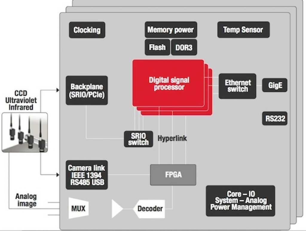
Figure 3. A typical image processing system
Conclusion
For many years, multicore DSPs have shown their value in a wide variety of applications across a range of industries. Homogenous multicore DSP devices have frequently been the choice of designers of systems requiring compute-intensive signal processing within a limited power budget and confined to a compact physical space. TI’s C6657/5/4 DSPs offer exceptional computational performance, a wide selection of I/O interfaces, expansive memory space and other key features integrated into hardware to support the high–performance needs of industrial inspection systems (Figure 4).
Figure 4. Comparison of devices in C665x family
The simplicity of developing a software-defined imaging system in a high-level language like C on DSP cores accelerates the implementation of new and innovative algorithms and reduces customers’ time-to-market.