A bit more than a year ago, Alliance member CEVA unveiled its MM3101 image and embedded vision processing core. Several months later, Alliance Platinum member Analog Devices introduced four new Blackfin SoCs, two of which contain the PVP (Pipelined Vision Processor) core. And now, newly minted Alliance member Tensilica has joined the party, too, with its scalable IVP (Imaging/Video DSP) IP core, now available for broad licensing subsequent to early customers' evaluations and design-ins that began last year, and after several years' worth of precursor core architecture definition and development work within Tensilica.
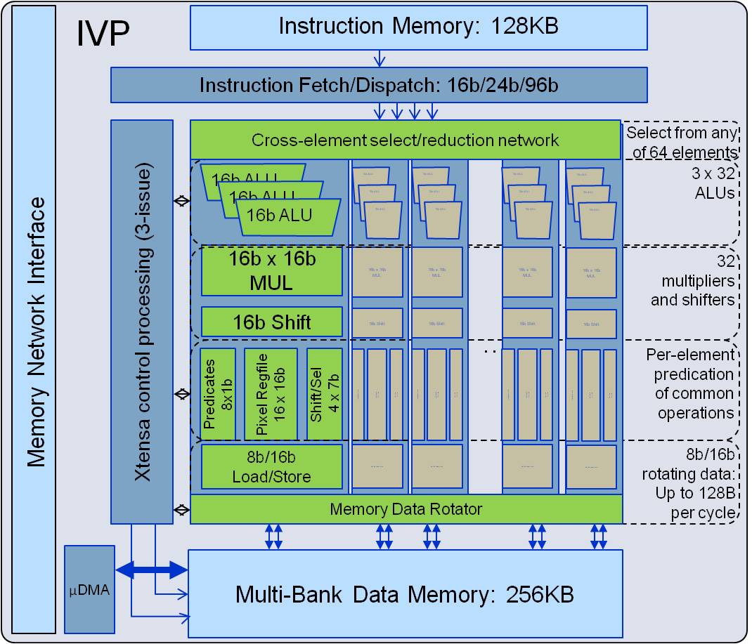
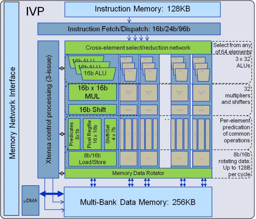
According to CTO and company founder Chris Rowan, the IPV has 10-20x the peak performance potential of most host CPUs ("the IVP is capable of over 130 billion 16-bit RISC-equivalent operations per second"); Tensilica also claims that the IPV delivers 2-4x the performance of any currently available merchant imaging DSP core. The IVP is based on a 4-way VLIW architecture, with a 32-way vector SIMD dataset. Acknowledging the importance of robust data flow to and from the core's processing nexus, Tensilica has provided the IPV with two 512-bit wide memory ports for local data RAM access of up to 64 16-bit pixels/cycle, along with a 512-bit wide DMA controller capable of up to 10 GBytes/second of throughput.
With respect to power efficiency, here's what Tensilica's press release promotes:
The IVP is extremely power efficient. As an example, for an IVP implemented in an automatic synthesis, place-and-route flow in 28nm HPM process, regular VT, a 32-bit integral image computation on 16b pixel data at 1080p30 consumes 10.8 mW. The integral image function is commonly used in applications such as face and object detection and gesture recognition.
And with respect to the core's raw performance potential:
IVP’s high performance is demonstrated by complex algorithm kernels such as motion search and normalized cross-correlation, commonly used in high-precision block and feature matching and optical flow. For a smart motion search on 16-bit data over a 1920×1080 frame with 256×16 pixel search range and 9×3 pixel block size, IVP can achieve a rate of 142 sums of absolute differences per cycle. In addition, a normalized cross-correlation function on 16-bit pixel data with 32-bit accuracy achieves 1 million 8×8 blocks per second.
The CPU core itself is an application-tailored Xtensa control processor supporting "many imaging-specific operations to accelerate 8-, 16- and 32-bit pixel data types and video operation patterns." Also included (in the default configuration) are 32 "element engines," each engine containing three 16-bit ALUs, a 16×16 bit multiply-add block, a 16-bit variable shifter, dual 16-bit or 8-bit load/store blocks, and various registers. As with other Tensilica processor cores, the IPV "can be further customized using Tensilica’s patented processor-generation system." And "it employs the C programming model common among all Tensilica DPUs (dataplane processors)," for straightforward porting of potential customers' existing imaging and embedded vision software.
Tensilica will be demonstrating the IPV later this month at the Mobile World Congress show, running as a prototype inside a Xilinx Virtex7 FPGA and on that Alliance Platinum member's evaluation board. For a full picture of the IPV, make sure you also check out the press releases from Tensilica's partner companies Almalence, Dream Chip Technologies, Irida Labs, and Morpho.