By Sateesh Reddy Jonnalagada and Vamsi Krishna
Xilinx Corporation
Embedded vision applications deal with a lot of data; a single 1080p60 (1920×1080 pixel per frame, 60 frames per second) 24-bit color video stream requires nearly 3 Gbps of bandwidth, and 8-bit alpha (transparency) or 3-D depth data further amplifies the payload by 33% in each case. Transferring that data from one node to another quickly and reliably is critical to robust system operation. As such, advanced interconnect technologies such as Xilinx's AXI are valuable in embedded vision designs. This is a reprint of a Xilinx-published application note, which is also available here (2.1 MB PDF).
This application note covers the design considerations of a video system using the performance features of the LogiCORETM IP Advanced eXtensible Interface (AXI) Interconnect core. The design focuses on high system throughput using approximately 80% of DDR memory bandwidth through the AXI Interconnect core with FMAX and area optimizations in certain portions of the design.
The design uses eight AXI video direct memory access (VDMA) engines to simultaneously move 16 streams (eight transmit video streams and eight receive video streams), each in 1920 x 1080 pixel format at 60 or 75 Hz refresh rates, and up to 32 data bits per pixel. Each VDMA is driven from a video test pattern generator (TPG) with a video timing controller (VTC) block to set up the necessary video timing signals. Data read by each AXI VDMA is sent to a common on-screen display (OSD) core capable of multiplexing or overlaying multiple video streams to a single output video stream. The output of the OSD core drives the onboard high-definition media interface (HDMI) video display interface through the color space converter.
The performance monitor block is added to capture DDR performance metrics. DDR traffic is passed through the AXI Interconnect to move 16 video streams over 8 VDMA pipelines. All 16 video streams moved by the AXI VDMA blocks are buffered through a shared DDR3 SDRAM memory and are controlled by a MicroBlazeTM processor.
The reference system is targeted for the Kintex-7 FPGA XC7K325TFFG900-1 on the Xilinx KC705 evaluation board (revision C or D) (Reference 1).
Included Systems
The reference design is created and built using version 13.4 of the Xilinx Platform Studio (XPS) tool, which is part of the ISE® Design Suite: System Edition. XPS helps simplify the task of instantiating, configuring, and connecting IP blocks together to form complex embedded systems. The design also includes software built using the Xilinx Software Development Kit (SDK). The software runs on the MicroBlaze processor subsystem and implements control, status, and monitoring functions. Complete XPS and SDK project files are provided with this application note to allow the user to examine and rebuild the design or to use it as a template for starting a new design.
Introduction
High-performance video systems can be created using Xilinx AXI IP. The use of AXI Interconnect, Memory Interface Generator (MIG), and VDMA IP blocks can form the core of video systems capable of handling multiple video streams and frame buffers sharing a common DDR3 SDRAM memory. AXI is a standardized IP interface protocol based on the Advanced Microcontroller Bus Architecture (AMBA®) specification. The AXI interfaces used in the reference design consist of AXI4, AXI4-Lite, and AXI4-Stream interfaces as described in the AMBA AXI4 specifications (Reference 2). These interfaces provide a common IP interface protocol framework around which to build the design.
Together, the AXI interconnect and AXI MIG implement a high-bandwidth, multi-ported memory controller (MPMC) for use in applications where multiple devices share a common memory controller. This is a requirement in many video, embedded, and communications applications where data from multiple sources moves through a common memory device, typically DDR3 SDRAM.
AXI VDMA implements a high-performance, video-optimized DMA engine with frame buffering, scatter gather, and two-dimensional (2D) DMA features. AXI VDMA transfers video data streams to or from memory and operates under dynamic software control or static configuration modes.
A clock generator and processor system reset block supplies clocks and resets throughout the system. High-level control of the system is provided by an embedded MicroBlaze processor subsystem containing I/O peripherals and processor support IP. To optimize the system to balance performance and area, multiple AXI Interconnect blocks are used to implement segmented/hierarchical AXI Interconnect networks with each AXI Interconnect block individually tuned and optimized.
Hardware Requirements
The hardware requirements for this reference system are:
- Xilinx KC705 evaluation board (revision C or D)
- Two USB Type-A to Mini-B 5-pin cables
- HDMI to DVI cable
- Display monitor supporting 1920 x 1080 pixel resolution up to 75 frames/sec (The reference design was tested using a Dell P2210 monitor)
The installed software tool requirements for building and downloading this reference system are:
- Xilinx Platform Studio 13.4
- ISE Design Suite 13.4
- SDK 13.4
Reference Design Specifics
In addition to the MicroBlaze processor, the reference design includes these cores:
- MDM
- LMB block RAM
- AXI_INTERCONNECT
- AXI2AXI Connector
- CLOCK GENERATOR
- PROC_SYS_RESET
- AXI_UARTLITE
- AXI IIC
- AXI_INTC
- AXI_7SERIES_DDRX
- AXI_BRAM
- AXI_VTC
- AXI_TPG
- AXI_VDMA
- AXI_PERFORMANCE_MONITOR
- AXI_OSD
- csc_rgb_to_ycrcb422
- HDMI_OUT IP
Figure 1 and Table 1 show a block diagram and address map of the system, respectively.

Figure 1. Reference System Block Diagram
Table 1. Reference System Address Map
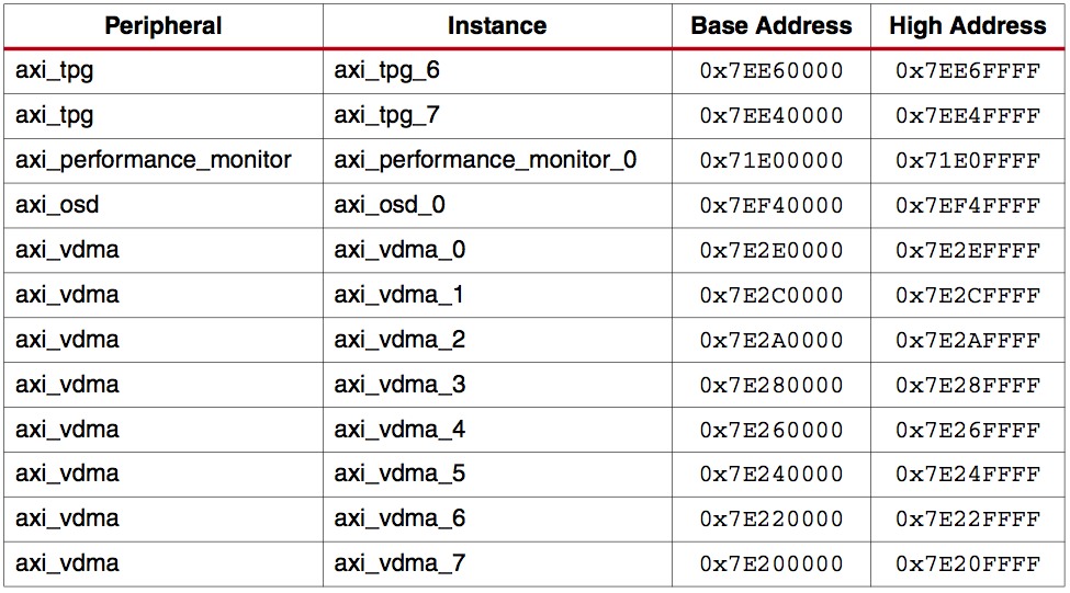
Table 1. Reference System Address Map (Cont’d)
Hardware System Specifics
This section describes the high-level features of the reference design, including how to configure the main IP blocks. Information about useful IP features, performance/area trade-offs, and other configuration information is also provided. This information is applied to a video system, but the principles used to optimize the system performance apply to a wide range of high-performance AXI systems. For information about AXI system optimization and design trade-offs, see AXI Reference Guide (Reference 3).
This application note assumes the user has some general knowledge of XPS. See EDK Concepts, Tools, and Techniques: A Hands-On Guide to Effective Embedded System Design (Reference 4) for more information about the XPS tools.
Video-Related IP
The reference design implements eight video pipelines each running at a 1920 x 1080 pixel format at 60 or 75 frames/sec. Each picture consists of four bytes per pixel to represent an upper bound for high-quality video streams like RBGA (with alpha channel information). Each video pipeline running at 60 frames/sec requires a bandwidth of 497.7 MB/s (~4 Gb/s) whereas at 75 frames/sec, each video pipeline requires a bandwidth of 622 MB/s (~5 Gb/s).
Note: The source code supplied with the reference design is for 1920 x 1080 pixels running at 75 Hz. To operate the same design at 60 Hz, the user should change the sixth port input frequency of the clock generator to 148000000 in the microprocessor hardware specification (MHS) file and run the design.
The video traffic is generated by TPG IP cores and displayed by the OSD core. The total aggregate read/write bandwidth generated is equivalent to 16 video streams requiring 9.9538 GB/s (7.96 Gb/s).
This application note demonstrates AXI system performance using 16 high-definition video streams. At a minimum, video systems must include a source, some internal processing, and a destination. There can be multiple stages internally using a variety of IP modules. The canonical video system in Figure 2 shows that most video systems consist of input, pre-processing, main processing, post-processing, and output stages. Many of the video stages illustrated require memory access at video rates. Video data goes in or out of memory according to the requirements of internal processing stages. In this application note, a series of test pattern generators create the internal IP block memory traffic to simulate typical conditions.
Figure 2. Typical Video System
AXI Interconnects
This design contains multiple AXI Interconnects each tuned to balance for throughput, area, and timing considerations (see LogiCORE IP AXI Interconnect Product Specification (v1.05.a) (Reference 5). The AXI_MM0, AXI_MM1, and AXI_MM2 instances are used for high-speed masters and slaves that include high throughput and high FMAX optimizations. The AXI_MM0, AXI_MM1, and AXI_MM2 interconnects are optimized for higher throughput. They are used to buffer frame data generated by the TPG and to access the same data from the buffer through the VDMA to display on the LCD. The AXI_Lite and AXI_Lite_Video Interconnect instances are generally optimized for area. They are used by the processor to access slave registers and to write to the VDMA register space for control of the AXI VDMA. The AXI VDMA operation and its register descriptions are described in detail in LogiCORE IP AXI Video Direct Memory Access (axi_vdma) (v3.01.a) data sheet (Reference 6).
AXI Interconnect (AXI_MM Instance)
This AXI Interconnect instance provides the highest FMAX and throughput for the design by having a 512-bit core data width and running at 200 MHz. The AXI Interconnect core data width and clock frequency match the capabilities of the attached AXI MIG so that width and clock converters between them are not needed. Sizing the AXI Interconnect core data width and clock frequency below the native width and clock frequency of the memory controller creates a system bandwidth bottleneck in the system. To help meet the timing requirements of a 512-bit AXI interface at 200 MHz, a rank of register slices are enabled between AXI_MM Interconnect and AXI MIG. Together, AXI Interconnect and AXI MIG form an 18-port AXI MPMC connected to MicroBlaze processor instruction cache (ICache) and data cache (DCache) ports, eight AXI VDMA MM2S ports, and eight AXI VDMA S2MM ports. The configuration of this AXI Interconnect is consistent with the system performance optimization recommendations for an AXI MPMC based system as described in the AXI Reference Guide (Reference 3).
AXI VDMA Instances
The AXI VDMA core is designed to provide video read/write transfer capabilities from the AXI4 domain to the AXI4-Stream domain, and vice versa. The AXI VDMA provides high-speed data movement between system memory and AXI4-Stream based target video IP. AXI4 interfaces are used for the high-speed data movement and buffer descriptor fetches across the AXI Interconnect.
The AXI VDMA core incorporates video-specific functionality, i.e., Gen-Lock and Frame Sync, for fully synchronized frame DMA operations and 2D DMA transfers. In addition to synchronization, frame store numbers and scatter gather or register direct mode operations are available for ease-of-control by the central processor.
In this design, the AXI VDMA scatter gather feature is not used because the system could be implemented sufficiently using the simpler register direct mode of AXI VDMA, which would remove the area cost of the scatter gather feature. Scatter gather should only be enabled if the system requires relatively complex software control of the AXI VDMA operations.
Initialization, status, and management registers in the AXI VDMA core are accessed through an AXI4-Lite slave interface.
This design uses eight instances of AXI VDMA, each using two 64-bit interfaces toward the AXI4 memory map and two 32-bit interfaces toward the streaming side. The upsizer in the VDMA is used to convert 32-bit transactions from the streaming side to 64-bit wide transactions to the memory map side of the VDMA core. Similarly, downsizers are used to convert 64-bit memory-mapped transactions to 32-bit streaming side transactions.
The 64-bit wide MM2S and S2MM interfaces from the AXI VDMA instances are connected to the AXI_MM instance of the AXI Interconnect. The masters run at 148.5 MHz (60 Hz frame rate)/185 MHz (75 Hz frame rate) (video clock), which require asynchronous clock converters to the 200 MHz AXI Interconnect core frequency. Upsizers in the AXI Interconnect are used to convert 64-bit transactions from the AXI VDMA to 512-bit wide transactions to the AXI Interconnect core.
For maximum throughput for the AXI VDMA instances, the maximum burst length is set to 256. In addition, the master interfaces have a read and write issuance of 4 and a read and write FIFO depth of 512 to maximize throughput. These settings all follow performance recommendations for AXI endpoint masters as described in the AXI Reference Guide (Reference 3).
In addition, line buffers inside the AXI VDMA for the read and write sides are set to 1K deep, and the store and forward features of the AXI VDMA are enabled on both channels to improve system performance and reduce the risk of system throttling. See the LogiCORE IP AXI Video Direct Memory Access (axi_vdma) (v3.01.a) data sheet (Reference 6) for more information.
If the design sets the parameter C_PRMRY_IS_ACLK_ASYNC to 1, follow these steps:
- Right-click on the core instance and select Make This IP Local to make the pcore local to the XPS project.
- Navigate to the pcores/axi_vdma_v5_00_a/data/ directory.
- Open the axi_vdma_2_1_0.tcl file.
-
Comment out any lines from 77 to 136 in the TCL file that incorrectly constrain signals in the same clock domain. For example, if the core is set to asynchronous mode (C_PRMRY_IS_ACLK_ASYNC=1) and m_axi_mm2s_aclk and s_axi_lite_aclk use the same clock source, comment out these timing ignore (TIG) constraints:
puts $outputFile "TIMESPEC TS_${instname}_from_s_axi_lite_aclk_to_m_axi_mm2s_aclk = FROM \"s_axi_lite_aclk\" TO \"m_axi_mm2s_aclk\" TIG;"
puts $outputFile "TIMESPEC TS_${instname}_from_m_axi_mm2s_aclk_to_s_axi_lite_aclk = FROM \"m_axi_mm2s_aclk\" TO \"s_axi_lite_aclk\" TIG;"
- Save the file.
- In XPS, select Project and click Rescan User Repositories.
MicroBlaze Processor ICache and DCache
The MicroBlaze processor ICache and DCache masters are connected to the AXI Interconnect and run at 100 MHz because the MicroBlaze processor runs a software application from main memory that sets up and monitors the video pipelines. Running the MicroBlaze processor at this frequency helps timing and area.
See the MicroBlaze Processor Reference Guide: Embedded Development Kit EDK 13.4 (Reference 7) for more information. The 100 MHz clock setting ensures that synchronous integer ratio clock converters in the AXI Interconnect can be used, which offers lower latency and less area than asynchronous converters.
AXI_7SERIES_DDRX
The single slave connected to the AXI Interconnect is the axi_7series_ddrx memory controller (a block that integrates the MIG tool into XPS). The memory controller’s AXI Interface is 512 bits wide running at 200 MHz and disables narrow burst support for optimal throughput and timing. This configuration matches the native AXI interface clock and width corresponding to a 64-bit DDR3 DIMM at 800 MHz memory clock, which is the maximum performance of the memory controller for a Kintex-7 device in -1 speed grade.
The slave interface has a read/write issuance of eight. Register slices are enabled to ensure that the interface meets timing at 200 MHz. These settings help ensure that a high degree of transaction pipelining is active to improve system throughput. See the 7 Series FPGAs Memory Interface Solutions User Guide (Reference 8) for more information about the memory controller.
AXI Interconnect (AXI_Lite, AXI_Lite_Video)
The MicroBlaze processor data peripheral (DP) interface master writes and reads to all AXI4-Lite slave registers in the design for control and status information.
These interconnects are 32 bits and do not require high FMAX and throughput. Therefore, they are connected to a slower FMAX portion of the design by a separate AXI Interconnect.
Because there are more than 16 AXI4-Lite slave interfaces in the design, AXI2AXI connectors and additional AXI Interconnect instances are required to allow the processor to access all the AXI4-Lite interfaces in the system.
The AXI_Lite and AXI_Lite_Video AXI Interconnect blocks are configured for shared-access mode because high throughput is not required in this portion of the design. Therefore, area can be optimized over performance on these interconnect blocks. Also, these two interconnects are clocked at 50 MHz to ensure that synchronous integer ratio clock converters in the AXI Interconnect can be used, which offer lower latency and less area than asynchronous clock converters.
AXI_Lite Interconnect
The slaves on the AXI_Lite Interconnect are for MDM, AXI_UARTLITE, AXI_IIC, AXI_INTC, AXI_VTC (two instances), AXI OSD, and the slave AXI2AXI connectors to the AXI_Lite_Video interconnect.
AXI_Lite_Video Interconnect
An AXI2AXI connector connects the AXI_Lite Interconnect to the AXI_Lite_Video Interconnect as a master. The slaves on this AXI Interconnect are AXI_TPG (eight instances) and the AXI VDMA slave interface (eight instances).
AXI VTC
The AXI VTC is a general-purpose video timing generator and detector. The input side of this core automatically detects horizontal and vertical synchronization pulses, polarity, blanking timing, and active video pixels. The output side of the core generates the horizontal and vertical blanking and synchronization pulses used in a standard video system including support for programmable pulse polarity.
The AXI VTC contains an AXI4-Lite Interface to access slave registers from a processor. For more information about the AXI VTC, see the LogiCORE IP Video Timing Controller v3.0 data sheet (Reference 9).
In this design, two AXI VTC instances are used without detection. The first instance is used for the video input portion of the video pipelines. The second instance is used for the AXI OSD, which is the read portion of the video pipelines.
The Video Timing Controller v3.0 core is provided under license and can be generated using the CORE GeneratorTM tool v13.2 or higher.
AXI TPG
The AXI TPG contains an AXI4-Lite Interface to access slave control registers from a processor.
In this reference design, the video traffic to DDR3 memory is generated by a series of TPGs. Each TPG block can generate several video test patterns that are commonly used in the video industry for verification and testing. In the reference design, the TPG is used as a replacement for other video IP because only the amount of traffic generated to demonstrate the performance of the system is of interest. The control software demonstrates generation of flat colors, color bars, horizontal and vertical burst patterns, and the generation of zone plates. No matter which test pattern is chosen, the amount of data generated is the same, namely, 1080p HD video. For example, an RGBA (32-bit), 1080p60 pattern generates 497.7 MB/s, which is a nearly 4 Gb/s data stream. Similarly, an RGBA (32-bit), 1920 x 1080 pixel pattern at a 75 Hz frame rate generates 622 MB/s, which is a nearly 5 Gb/s data stream.
Several operating modes are accessible through software control. In this application note, the TPG always generates a test pattern that could be one of flat colors, color bars, horizontal ramp, vertical ramp, or zoneplates. These patterns are meant for testing purposes only and are not calibrated to broadcast industry standards.
AXI OSD
The OSD LogiCORE IP provides a flexible video-processing block for alpha blending, compositing up to eight independent layers, and generating simple text and graphics capable of handling images up to 4K x 4K sizes in YUVA 4:4:4 or RGBA image formats in 8, 10, or 12 bits per color component. In this application note, the OSD blends the eight video streams as separate display layers. Because the video streams generated by the TPG cores are enabled through software control, the display shows the blended layers on top of each other. Figure 3 shows a three-level block diagram of the OSD core.
Figure 3. Sample Three-Layer OSD Core Block Diagram
The AXI OSD contains an AXI4-Lite interface to access the slave registers from a processor. For more information about the AXI OSD, see the LogiCORE IP Video On-Screen Display v2.0 data sheet (Reference 10).
The Video On-Screen Display core is provided under the SignOnce IP site license and can be generated using the CORE Generator tool, which is a part of the Xilinx ISE Design Suite software tool.
A simulation evaluation license for the core is shipped with the CORE Generator system. To access the full functionality of the core, including FPGA bit-stream generation, a full license must be obtained from Xilinx.
AXI Performance Monitor
The AXI performance monitor core (AXI PERFORMANCE MONITOR) measures throughput for a DDR3 memory connected to the AXI Interconnect. The processor accesses the AXI performance monitor core registers through a slave AXI4-Lite interface contained in the core. The AXI performance monitor core only monitors the read and write channels between the AXI slave and the AXI Interconnect. The core does not modify or change any of the AXI transactions it is monitoring. The core also calculates the glass-to-glass delay of the system by connecting appropriate signals to it.
Note: In this application note, glass-to-glass delay is defined as the number of clock cycles consumed to display a frame from the TPG (video source) on an LCD screen (video sync).
Several signals must be connected in the system to measure the throughput. The DDR slave interconnect (AXI_MM) is connected to one of the four slots of the monitor. In addition to these, the AXI_Lite bus interface is connected to access the core registers by the processor. In addition to the signals of these two bus interfaces, the core clock (the higher of the two bus interface clock frequencies) must be connected. To evaluate the glass-to-glass delay of the system “Vid_clk”, “Vtc0_Fsync”, “Vsync_osd”, “Tpg_Active_video_in”, “Tpg_Data”, “Osd_Active_Video_In”, and “Osd_data” are also connected. The Fsync signal generated by the VTC and the Vsync signal generated by the color space converter are used to evaluate glass-to-glass delay.
The core can measure performance metrics such as total read byte count, write byte count, read requests, write requests, and write responses. Count start and count end conditions come from the processor through the register interface. The global clock counter of the core measures the number of clocks between the count start and count end events. The counters used for the performance monitor can be configured for 32 or 64 bits through the register interface. Final user-selectable metrics can also be read through the register interface.
In this application note, the DDR3 slave is connected to one of the slots of the AXI performance monitor core to measure the throughput of the core. Valid, ready, strobe, and other AXI signals connected to the performance monitor slots are used to enable various counters for measuring events on the bus.
Software Applications: AXI VDMA DISPLAY Application
The software application starts up the video pipelines allowing the user to examine bandwidth in real time and display separate layers or alpha blend all layers on the LCD screen.
Application-level software for controlling the system is written in C using the provided drivers for each IP. The programmer’s model for each IP describes the particular API used by the drivers. Alternatively, application software can be written to use the IP control registers directly and handle the interrupts at the application level, but using the provided drivers and a layer of control at the application level is a far more convenient option.
The application software in the reference design performs these actions:
- The software application first resets the HDMI port on the KC705 board through the IIC interface.
- The TPG instances are set to write a default gray pattern that does not start until the AXI VTC instances are started.
- The AXI VDMA instances are started, which consists of the processor writing into its registers. The program then starts the read/write channels to begin the transfers for the VDMA instances.
- The AXI VTC instances are started with 1920 x 1080 pixels (75 Hz) timing configuration.
-
The AXI OSD is configured for 1920 x 1080 resolution output. The eight TPG instances in the design are configured to write:
• Color bars (layer 0)
• Zone plate patterns (layer 1)
• Vertical bars (layer 2)
• Horizontal bars (layer 3)
• Tartan bars (layer 4)
• Flat red (layer 5)
• Flat green (layer 6)
• Flat blue (layer 7)
After the initial setup sequence, the user can choose to view a certain layer by selecting a number (option 0–7). When the number of a particular layer is selected, the OSD registers are modified to make the alpha blending on that particular layer be the highest value, while the others are at the smallest. When option 8 is selected (alpha blending all layers), different values are given to the alpha blending register for each layer to show all layers on the LCD screen at the same time. Option 9 reads performance metrics from the core and option d displays the glass-to-glass delay consumed by the system.
Executing the Reference Design in Hardware
This section provides instructions to execute the reference design in hardware. This reference design runs on the KC705 board shown in Figure 4.
Figure 4. KC705 Board
In these instructions, numbers in parentheses correspond to callout numbers in Figure 4. Not all callout numbers are referenced.
- Connect a USB cable from the host PC to the USB JTAG port (6). Ensure the appropriate device drivers are installed.
- Connect a second USB cable from the host PC to the USB UART port (12). Ensure that the USB UART drivers described in Hardware Requirements have been installed.
- Connect the KC705 HDMI connector (18) to a video monitor capable of displaying a 1920 x 1080 resolution and displaying up to 75 Hz video signal.
- Connect a power supply cable.
- Set power ON (27).
-
Start a terminal program (e.g., HyperTerminal) on the host PC with these settings:
• Baud Rate: 9600
• Data Bits: 8
• Parity: None
• Stop Bits: 1
• Flow Control: None
Executing the Reference System Using the Pre-Built Bitstream and the Compiled Software Application
These are the steps to execute the system using files in the ready_for_download directory of the <unzip_dir>/kc705_video_8x_pipeline/ directory:
-
In a command shell or terminal window, change directories to the ready_for_download directory. Move into one of the directories 60Hz or 75Hz (75Hz is shown in this example):
% cd <unzip dir>/kc705_video_8x_pipeline/ready_for_download/75Hz
-
Invoke the Xilinx Microprocessor Debugger (XMD) tool:
% xmd
-
Download the bitstream inside XMD:
XMD% fpga -f download.bit
-
Connect to the processor inside XMD:
XMD% connect mb mdm
-
Download the processor code (ELF) file:
XMD% dow axi_vdma_display.elf
-
Run the software:
XMD% run
Results from Running Hardware and Software
The Dell P2210 LCD monitor connected to the KC705 board displays a color bar pattern, and the HyperTerminal screen displays the output shown in Figure 5.
Figure 5. HyperTerminal Output
The user can choose one of the eleven options displayed on the HyperTerminal screen:
- 0 = Color bars (layer 0)
- 1 = Zoneplate patterns (layer 1)
- 2 = Vertical ramp (layer 2)
- 3 = Horizontal ramp (layer 3)
- 4 = Tartan bars (layer 4)
- 5 = Flat red (layer 5)
- 6 = Flat green (layer 6)
- 7 = Flat blue (layer 7)
- 8 = Alpha blend of all layers simultaneously (layers 0–7)
- 9 = Real-time system performance (one second of transfers)
- d = Real-time system glass-to-glass delay of one frame
Performance
The AXI_MM interconnect is 512 bits running at 200 MHz. The theoretical maximum bandwidth on each channel is 12.8 GB/s.
The DDR3 PHY is set for 64 bits with a memory clock frequency of 800 MHz. The theoretical throughput on DDR3 is 12.8 GB/s, which is the total bandwidth available in the design.
Using option 9 of the software application should show this output (the numbers might vary slightly from the values shown):
———DDR3, AXI4 Slave Profile Summary……..
| Theoretical DDR Bandwidth | = 12800000000 bytes/sec |
| Practical DDR bandwidth | = 9975795872 bytes/sec |
|
Percentage of DDDR Bandwidth consumed by eight Video Pipelines (Approx.) |
= 77.9359% |
The total bandwidth is approximately 9,975 MB/s out of 12,800 MB/s, which is around 77% of the total theoretical bandwidth of the main memory.
Using option d of the software application should display this output:
Processing Time Per Frame (Glass to Glass delay) = 13.572015 ms
Note: The numbers might vary slightly from the values shown.
Building Hardware
This section covers rebuilding the hardware design.
Before rebuilding the project, the user must ensure that the licenses for AXI OSD and AXI VTC are installed. To obtain evaluation licenses for the AXI VTC or AXI OSD, refer to these websites:
- Xilinx Video Timing Controller (Reference 11)
- Xilinx On-Screen Display LogiCORE IP (Reference 12)
Note: The source code in the reference design only applies to the 75 Hz frame rate. The user can change the input frequency of the sixth clock port in the MHS file to 148000000 and generate a bitstream to operate in 60 Hz mode. The generated bitstream is at
<unzipdir>/kc705_video_8x_pipelne/HW/K7_MB_video_pipelines/implementation/download.bit
- Open kc705_video_8x_pipeline/HW/k7_MB_video_pipelines/system.xmp in XPS.
- Select Hardware > Generate Bitstream to generate a bitstream for the system.
- Select Device Configuration > Update Bitstream to initialize the block RAM with a bootloop program. This ensures that the processor boots up with a stable program in memory.
Compiling Software in SDK
- Start SDK. In Linux, type xsdk to start SDK.
-
In the workspace launcher, select this workspace:
<unzip dir>/kc705_video_8x_pipeline/SW/SDK_Workspace
- Click OK.
- Set the repository by selecting Xilinx Tools > Repositories.
- For local repositories, click New….
- Change directories to <unzip dir>/kc705_video_8x_pipeline/SW/repository.
- Click OK.
- Import the board support package (BSP), hardware platform, and software applications by selecting File > Import > General > Existing Projects into the workspace.
- Click Next, then browse to <unzip dir>/kc705_video_8x_pipeline/SW.
- Click OK.
- Ensure that all checkboxes are selected (including axi_vdma_display and K7_MB_video_pipelines_hw_platform).
- Ensure that the associated software applications are selected.
- Click Finish.
The BSP and software applications compile at this step. The process takes 2 to 5 minutes. The user can now modify existing software applications and create new software applications in SDK.
Running the Hardware and Software through SDK
-
Select Xilinx Tools > Program FPGA.
Note: Ensure bootloop is used for microblaze_0.
- Click Program.
- In the Project Explorer window, right click and select axi_vdma_display > Run As > Launch on Hardware.
Design Characteristics
The reference design is implemented in a Kintex-7 FPGA (XC7K325TFFG900-1) using the ISE Design Suite: Embedded Edition 13.4.
The resources used are:
- Total LUTs used: 97,101 out of 203,800 (47%)
- Total I/Os used: 163 out of 500 (32%)
-
Total internal memory used:
• RAMB36E1s: 236 out of 445 (53%)
• RAMB18E1s: 57 out of 890 (6%)
Note: Device resource utilization results depend on the implementation tool versions. Exact results can vary. These numbers should be used as a guideline.
Reference Design
The reference design has been fully verified and tested on hardware. The design includes details on the various functions of the different modules. The interface has been successfully placed and routed at 200 MHz on the main AXI Interfaces to the memory controller using the ISE Design Suite 13.4.
The reference design files for this application note can be downloaded from:
https://secure.xilinx.com/webreg/clickthrough.do?cid=184421
The reference design matrix is shown in Table 2.
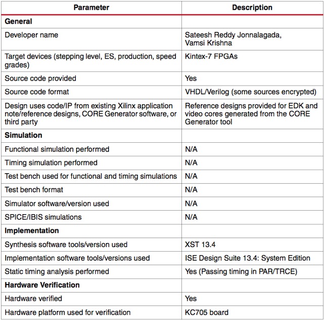
Table 2. Reference Design Matrix
Utilization and Performance
Table 3 shows device and utilization information.
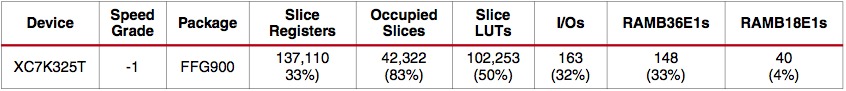
Table 3. Device and Utilization
Device resource utilization is detailed in Table 4 for the IP cores shown in Figure 1. The information in Table 4 is taken from the Design Summary tab in XPS under the Design Overview > Module Level Utilization report selection. The utilization information is approximate due to cross-boundary logic optimizations and logic sharing between modules.
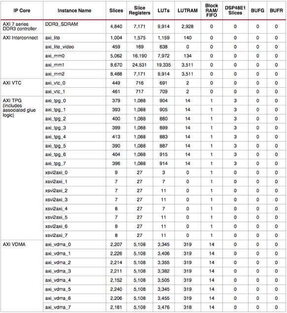
Table 4. Module Level Resource Utilization
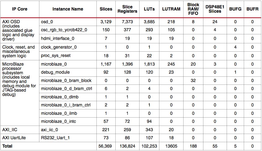
Table 4. Module Level Resource Utilization (Cont’d)
Table 5 summarizes the bandwidth calculations for the physical memory interface.

Table 5. DDR3 Memory Physical Interface Maximum Theoretical Bandwidth
Table 6 summarizes the total bandwidth of video data moved through memory.
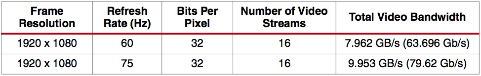
Table 6. Average Bandwidth Used for Video Traffic
Table 7 summarizes the percentage of the maximum theoretical bandwidth used by the video streams.
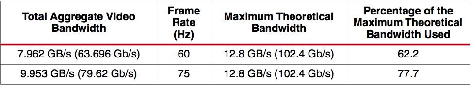
Table 7. Percentage of the Maximum Theoretical Bandwidth Used
Conclusion
This application note describes a video system using an AXI Interconnect core configured to operate at a bandwidth of approximately 10 GB/s. Eight video pipelines, each processing high-definition video streams of 1920 x 1080 pixels at 75 frames/sec are connected to the DDR memory through the AXI Interconnect. To meet high-performance design requirements, the DDR3 controller (DDR memory with an 800 MHz clock and 64-bit data width) is configured to utilize approximately eighty percent of its available bandwidth.
References
This application note uses the following references:
- UG810, KC705 Evaluation Board for the Kintex-7 FPGA User Guide
-
AMBA AXI4 specifications
http://infocenter.arm.com/help/index.jsp?topic=/com.arm.doc.set.amba/index.html - UG761, AXI Reference Guide
- UG683, EDK Concepts, Tools, and Techniques: A Hands-On Guide to Effective Embedded System Design (v13.4)
- DS768, LogiCORE IP AXI Interconnect Product Specification (v1.05.a)
- DS799, LogiCORE IP AXI Video Direct Memory Access (axi_vdma) Product Specification (v3.01.a)
- UG081, MicroBlaze Processor Reference Guide: Embedded Development Kit EDK 13.4
- UG586, 7 Series FPGAs Memory Interface Solutions User Guide
- DS857, LogiCORE IP Video Timing Controller v3.0 Product Specification
- DS837, LogiCORE IP Video On-Screen Display v2.0 Product Specification
-
Xilinx Video Timing Controller
http://www.xilinx.com/products/intellectual-property/EF-DI-VID-TIMING.htm -
Xilinx On-Screen Display LogiCORE IP
http://www.xilinx.com/products/intellectual-property/EF-DI-OSD.htm - UG111, Embedded System Tools Reference Manual: EDK v13.4