Before a still image or video stream can be analyzed, it must first be captured and transferred to the processing subsystem. Cameras, along with the interfaces that connect them to the remainder of the system, are therefore critical aspects of any computer vision design. This article provides an overview of camera interfaces, and discusses their evolutions and associated standards, both in general and with specific respect to particular applications. It also introduces an industry alliance available to help product creators incorporate robust vision capabilities into their designs.
Cameras, along with the processors and algorithms that analyze the images captured by them, are an integral part of any computer vision system. A variety of interface options, each with a corresponding set of strengths and shortcomings, exist for connecting cameras to the remainder of the design. And the options list isn't static; legacy standards (both de facto and official) lay the foundations for the emerging standards that follow them.
These interface options cover the connections between standalone cameras and systems, as well as and the links between both camera modules and image sensors and other ICs within an integrated system. Sometimes, camera interface requirements are by necessity application-specific. However, whenever possible, it's beneficial from volume cost amortization and other standpoints to be able to generalize these requirements across classes of applications. And performance, power consumption, cost, breadth of existing industry support (and future trends in this regard) and other factors are all key considerations to be explored and traded off as needed in any particular implementation.
In this article we will first discuss interface standards for industrial vision systems, then turn our attention to automotive-related standards, and conclude with a discussion of intra-system camera- and sensor-to-processor interfaces.
Industrial Vision
In the machine and industrial vision market segment, digital cameras are replacing their analog forebears and find use in diverse applications, including production processes (PCB inspection, glass surface inspection, robot control, etc.) and hyperspectral imaging. Digital cameras are expected to deliver long-term reliability, real-time capability, and exceptional image quality. And as imaging requirements have evolved, so too have fidelity, frame rates and resolution needs. Gone are the days of 15 Hz video captured at 1.3 Mpixels per frame. Today's cameras are capable of operating at hundreds of frames per second and deliver images beyond 20 Mpixels in resolution, along with improved color depth, low-light performance and other quality metrics.
Machine vision applications often require complicated image processing, therefore necessitating the transfer of uncompressed image data from the camera to the host computer. This requirement further increases the demand for robust, high bandwidth interfaces. And because many applications operate in assembly line, remote or other harsh environments, they drive additional requirements for long cable lengths, efficient power transmission, and reliable communication protocols. These sometimes-contending factors have contributed to the development of several different video interfaces to connect machine vision cameras to a processing unit.
In order to meet varying performance and other requirements while maintaining a level of standardization, manufacturers of machine vision hardware and software have developed an open vision interfacing standard called the Generic Interface for Cameras (GenICam), which is hosted by the EMVA (European Machine Vision Association). The intention of GenICam is to insure that the software API (application programming interface) remains consistent regardless of the hardware interface in use. This commonality makes it possible to combine any compliant camera with any compliant application. The GenICam standard covers a variety of old-to-new interfaces, including IEEE 1394, Camera Link, CoaXPress, GigE Vision and USB Vision. The latter two interfaces are the most recent, and address modern requirements for video transmission, device interoperability, and camera configuration and control.
GigE Vision uses gigabit Ethernet as its physical layer for image data transfer. The GigE Vision standard adds two application layer protocols to the UDP protocol stack: GVCP (the GigE Vision Control Protocol) and GVSP (the GigE Vision Stream Protocol). These protocols both avoid the overhead that comes with TCP-based protocols and deliver the needed reliability (IP packet retransmission, for example) to UDP, together making reliable data rates of up to 120 MBytes/sec feasible. The interface's Ethernet framework enables the creation of camera networks, which makes GigE Vision the ideal interface for multi-camera applications capable of up to 100 m cable lengths between network nodes.
The most recent version of the standard, GigE Vision 2.0 introduced in 2011, delivers additional features such as precise PTP (Precision Time Protocol) time stamps and broadcast triggering. The latter allows users to simultaneously trigger cameras in multi-camera applications over the existing Ethernet cable, without need for additional I/O trigger cables, and in a very precise manner down to a few microseconds of latency. And many GigE Vision-compliant cameras offer built-in PoE (Power over Ethernet) capabilities, negating the need for a local power supply. GigE Vision cameras can operate via any standard Gigabit Ethernet port ranging from a standard desktop PC to embedded processing board; GigE add-in cards are also available that are specifically designed for GigE Vision (providing a PoE supply or enhanced I/O capabilities, for example). And multi-port GigE cards allow operating up to four GigE Vision cameras with full bandwidth using a single PCIe add-in slot.
If more bandwidth per camera is required, USB3 Vision may be an attractive alternative. Introduced in 2013, this standard uses USB 3.0 as the underlying transmission protocol and offers image data rates up to 350 MBytes/s. Prior to the publication of the USB3 Vision specification, an industry standard for USB devices in the image processing industry did not exist. Various camera manufactures released proprietary solutions based around the USB 2.0 interface used on in mass market. USB 2.0 capabilities were generally insufficient, however, to ensure adequate component stability and durability, along with overall solution robustness, at the levels required for industrial applications.
Today, in contrast, virtually every new PC and embedded processing board is equipped with USB 3.0 ports. USB3 Vision cameras can therefore be connected to a processing unit without additional hardware. And just as GigE Vision builds on top of UDP, USB3 Vision adds real-time capabilities and reliability to USB 3.0. The plug-and-play nature of USB 3.0 leads to straightforward integration of machine vision cameras into an application. However, USB3 cable lengths are not as long as is possible with GigE, and long USB3 cable spans can also be prone to radiating high EMI levels. Designers should be cognizant of these discrepancies when selecting a camera interface, determining whether data rate or transmission length is more important in their particular application.
ADAS and Autonomous Vehicles
ADAS (advanced driver assistance systems) and even more complex autonomous vehicles require the ability to interface to multiple cameras, located around the automobile and viewing both external and internal perspectives. These standalone cameras leverage commonly used traditional automotive interfaces such as:
- MOST (Media Oriented Systems Transport): A high-speed network implemented over either optical or electrical physical layers, MOST uses a ring topology.
- CAN (Controller Area Network): A low-speed (1 Mbit/s) network implemented over an electrical physical layer. CAN nodes connect as a multi-master bus.
- FlexRay: A medium-speed (10 Mbit/s) network implemented over an electrical physical layer. It can use either a ring or multi-master bus.
- IDB-1394 (the Intelligent Transportation Systems Data Bus Using IEEE1394 Technology): A (400 Mbit/s) high-speed network implemented over an electrical physical layer. It uses a daisy-chained topology.
- LVDS (Low-voltage Differential Signaling): A point-to point-technology that protocols such as Camera Link can use for control and data transfer purposes (Figure 1).
Figure 1. The Camera Link protocol can operate in a point-to-point fashion via LVDS technology.
Each of these automotive interfaces requires a PHY to convert between the LVCMOS interface signals and levels used by the processor and those required by the protocol. In the case of the MOST protocol, the PHY must also convert between the electrical to the optical domains. Should an All-Programmable SoC (single-chip FPGA plus CPU) find use as the processor, for example, either the PS (processing systems) or PL (programmable logic) portion of the chip can interface with the PHY. If the design employs the PS, in order to take advantage of included I/O peripherals such as the CAN interface, DDR memory in conjunction with DMA can then be leveraged to transfer image data to the PL portion of the device for further processing.
Each of these traditional automotive protocols delivers different bandwidth capabilities, which defines the resolution, frame rate and pixel size which the camera is capable of outputting. Video sent over CAN, for example, must often first be highly compressed, resulting in additional processing complexity to restore the image to adequate quality prior to further processing. More generally, network-based protocols are popular in automotive applications, since they reduce the number of interconnections required between the various nodes. This simplification factors into a reduction in overall vehicle mass, thereby improving fuel economy and cost. However, the network must deliver the bandwidth required to transfer image data between each camera and the processing nexus, along with delivering required latency.
The architecture of the network is very important, as different topologies will result in varying data transfer processing requirements. A bus topology, with the processor master addressing various camera slaves as required to obtain image data, can be the simplest approach. Daisy-chained and ring topologies are similar, with data simply passing from one node to the next if not intended for it. In fact, a daisy -chained topology can transform into a ring network if the end daisy-chained nodes are connected. However, the use of daisy-chained and ring topologies result in more complex per-node requirements to route and process messages.
Ethernet and Point-to-point
Speaking of networks, the earlier-discussed Ethernet-based interface for industrial vision also bears consideration in automotive applications. Broadcom, for example, originally developed the Ethernet-derived BroadR-Reach physical layer, with the goal of bringing cost-effective, high-bandwidth connectivity to vehicles. This 100 Mbps communications standard was later standardized as 100BASE-T1 in IEEE 802.3bw-2015 Clause 96. It transmits data over a single copper pair, with 3 bits per symbol, and supports full duplex mode, simultaneously transmitting in both directions. In June 2016, the IEEE P802.3bp working group subsequently also standardized 1000BASE-T1, bringing 1 Gbps bandwidth to low cost, single pair cabling.
Replacing traditional wiring with 100BASE-T1 connections delivers many conceptual advantages. Unshielded twisted pair cables along with smaller and more compact connectors that deliver data at 100 Mbps can reduce connectivity costs by up to 80 percent and cabling weight up to 30 percent versus traditional alternative approaches. However, since even a 1 Mpixel, 4:2:0, 30fps video stream consumes more than 3x the bandwidth available in a 100 Mbps link, it needs to be compressed prior to transmission. Typically H.264's more complex High 10 Intra, High 4:2:2 Intra, and High 4:4:4 Intra profiles find use for video compression, since these profiles support more bits per pixel. Also, these codec variants can operate without storing a full frame in memory due to their intra-only coding schemes, thereby removing the need for external DRAM and resulting in low-cost solutions that retain high quality.
BMW first introduced Ethernet in their cars in 2008 for software updates, diagnostics, and private links. In 2011, the company's scope expanded to additionally using Ethernet for infotainment and driver assist. BMW subsequently introduced Ethernet-based cameras for rear and surround view on the company's 2013 vehicle models. And at the Ethernet Technology Day in 2015, BMW announced that it had adopted Ethernet as the main system bus in new 7-series vehicles. Other automotive OEMs are quickly following BMW's lead: Jaguar Land Rover, VW, Audi, Porsche, and General Motors are today also in production with Ethernet-based systems.
On the other end of the implementation spectrum is a point-to-point connection implemented over LVDS. Such interfaces provide for a simple, high performance connection between the processor and each camera. The aggregate cost and complexity, however, are increased versus an alternative networked approach, due to the requiring cabling between each camera and the processing core. Once commonly used protocol implemented over LVDS is Camera Link, which serializes 28 bits of data across five LVDS channels (4 data, 1 clock). In its base configuration, this point-to-point interface is capable of supporting data rates at up 2.04 Gbps.
MIPI Alliance Standards
To this point in the article, we've discussed several application-focused examples of inter-system interfaces, which connect standalone cameras to distinct processing modules such as a computer. Now, we'll explore intra-system interfaces, intended to connect an image sensor or camera module to a locally located processor within the same system. Much of today's industry standardization effort in this area is spearheaded by the MIPI Alliance; the organization's CWG (Camera Working Group) brings together image sensor companies and application processor companies, along with test equipment and validation IP providers, to develop and advance various imaging and vision interface solutions.
MIPI has developed two different imaging architectures to address industry needs (Figure 2):
- MIPI CSI-2 is a purpose-built integrated architecture consisting of both application and transport layers, and supporting both MIPI's C-PHY and D-PHY physical layer designs. CSI-2 has achieved broad market adoption in mobile and mobile influenced products, and continues to evolve on a two-year cadence to meet various applications' imaging and vision needs.
- MIPI CSI-3 is an application stack developed to work with an existing UniPro transport network utilizing MIPI's M-PHY physical layer specification. The CSI-3 v1.1 specification was released in 2014, provides camera and video capabilities, and is stable with no further evolution planned at this time.
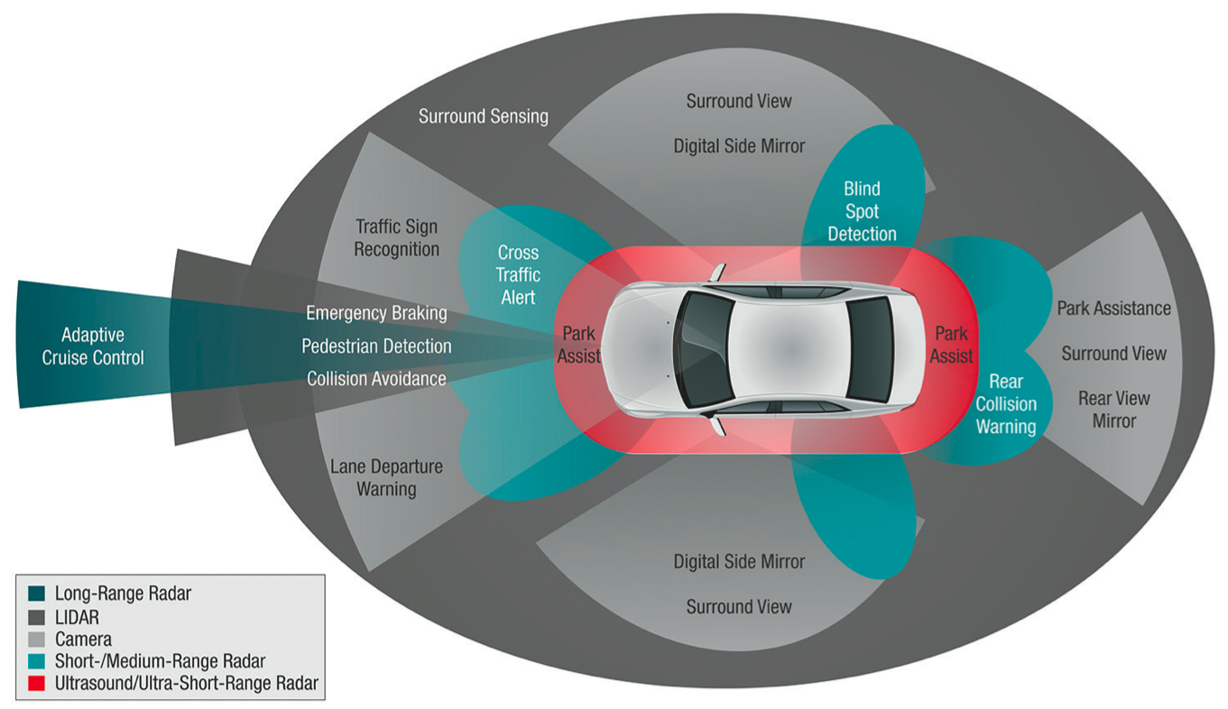
Figure 2. The MIPI Alliance's CSI-2 and CSI-3 specifications address varying transport and PHY requirements.
The CSI-2 v1.3 specification, finalized in 2014 and also referred to by MIPI as "Gen2", evolves beyond prior 6 Gbps/10 wire performance limitations (Figure 3). Its link performance gains can deliver enhanced system capabilities such as higher-resolution sensors, faster frame rates, expanded color depths, and HDR (high dynamic range) imaging enhancements. When used in conjunction with the C-PHY, CSI-2 v1.3 operates at up to 5.7 Gbps (2.5 Gsps), using a 3-wire embedded clock and data scheme, with lane scaling of +3. The C-PHY variant also uses innovating coding techniques to reduce channel toggle rate by a factor of 2.28x versus prior approaches.
Figure 3. "Gen2" CSI-2 v1.3 improves both link rate and power consumption metrics versus specification predecessors.
When used in conjunction with the D-PHY, CSI-2 v1.3 operates at up to 2.5 Gbps, using 4 wires (and lane scaling of +2) with differential data and a forwarded differential clock. The 35-40% power consumption reduction of CSI-2 v1.3-based image sensors versus precursors will be valuable in many applications. This reduced power consumption also translates into lower heat emissions, beneficial in medical applications that may involve direct contact with live tissue, such as high-definition "cold cam" imaging, for example.
An explanation of lane scaling follows: A MIPI CSI-2 over D-PHY link requires a minimum of 4 wires; 2 for the forwarded periodic clock, and 2 for the data lane. The link may realize higher bandwidth by scaling the data lanes with multiples of 2 data wires. For instance, high performance image sensors often use 2 wires for the clock and 8 wires to realize 4 data lanes. Similarly, a MIPI CSI-2 over C-PHY link requires a minimum of 3 wires, for the embedded clock and data. The link may realize higher bandwidth by scaling the embedded clock and data lanes with multiples of 3 wires. For instance, high performance image sensors often use 9 wires to realize 3 lanes. Moreover the CSI-2 over C-PHY link utilizes encoding to realize 2.28x bandwidth gain versus the channel toggle rate. For instance, a 3.5 GSps CSI-2 over C-PHY lane delivers 8 Gsps of effective bandwidth.
An explanation of why the reduced toggle rate of the C-PHY version of CSI-2 v1.3 is important follows: Image sensors often use process nodes that are a few generations older than those employed by application processors. Therefore, a reduced toggle rate (i.e. switching rate) may be beneficial with these older process node technologies.
CS1-2 v2.0 and Successors
The latest published CSI-2 standard is v2.0, released in 2016 and also referred to as "Gen3". When used in conjunction with the C-PHY, CSI-2 v2.0 operates at up to 8 Gbps (3.5 Gsps), as before leveraging a 3-wire embedded clock and data scheme with lane scaling of +3. And when used in conjunction with the D-PHY, CSI-2 v2.0 operates at up to 4.5 Gbps, again leveraging 4 wires and lane scaling of +2. CSI-2 v2.0 also delivers five other key imaging enhancements versus its specification predecessors.
RAW-16 and RAW-20 Support
CSI-2 v2.0 introduces RAW-16 and RAW-20 color depth imaging capabilities derived from scaling the prior-generation RAW-8 and RAW-10 pipeline architectures. Such advancements can significantly improve HDR and SNR (signal-to-noise ratio) capabilities for a variety of vision applications.
Enhanced Virtual Channels
The proliferation of image sensors, both standalone and coupled to aggregators, along with multi-exposure HDR imaging are driving the requirement for considerably higher VC (virtual channel) support on a variety of platforms. CSI-2 v2.0 provides much needed VC expansion from prior CSI-2 specification solutions, which were limited to 4 VCs (Figure 4). For example, if an ADAS-equipped or autonomous vehicle is equipped with three pairs of sensors, supporting short-, mid- and long-range viewing, and with each pair implementing both three-exposure HDR and IR (infrared) image capture capabilities, the system would require 24 VCs.
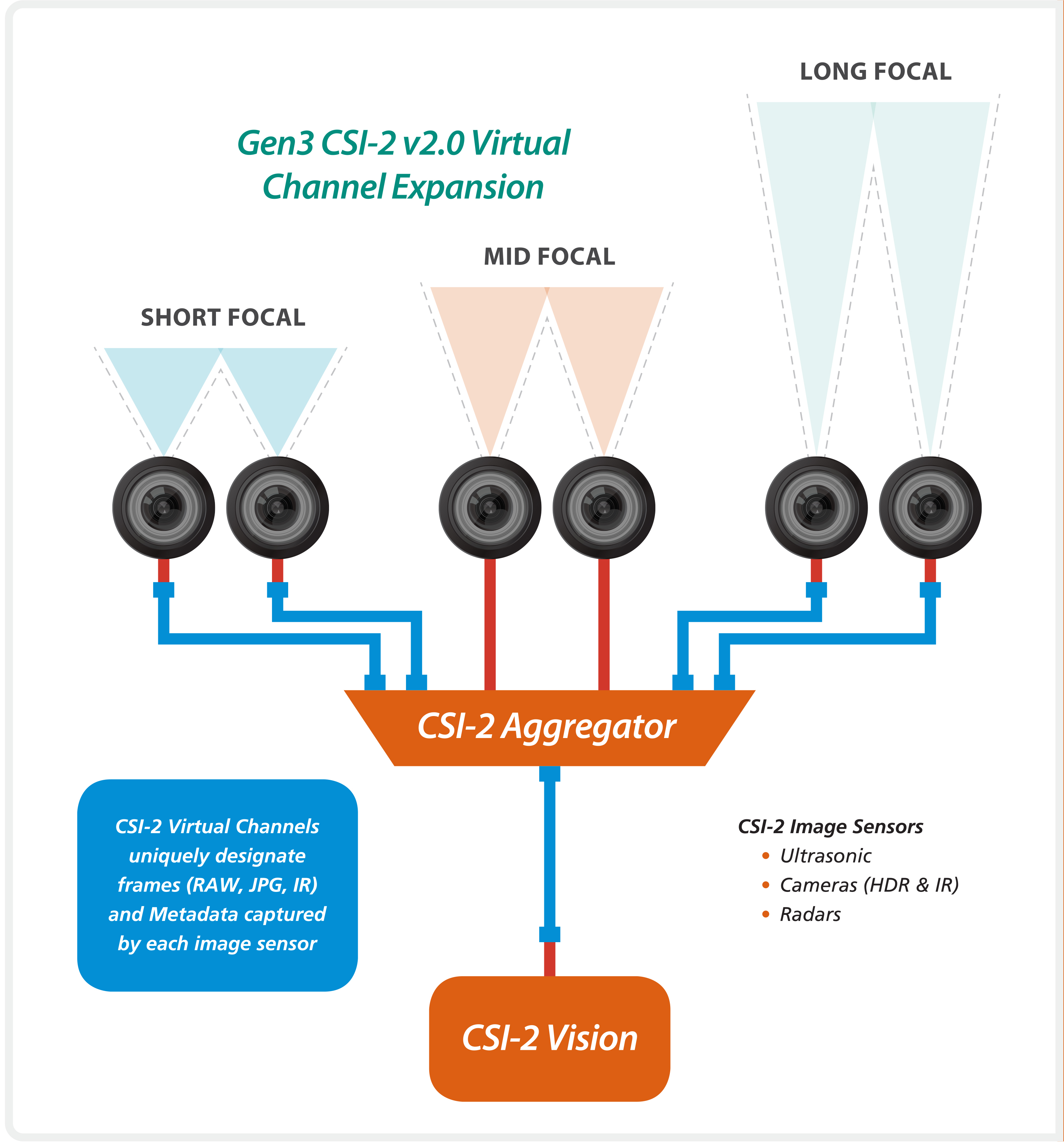
Figure 4. Expanded virtual channel support addresses increasingly common multi-camera configurations.
CSI-2 v2.0 over D-PHY now supports up to 16 VCs. In this particular physical layer implementation, the VC expansion also requires a newly architected ECC (error-correcting code) implementation in order to recover up to two bits' worth of information. Conversely, CSI-2 v2.0 over C-PHY directly supports up to 32 VCs, with a path to extend this support up to 1,024 VCs. Expanding VCs for CSI-2 2.0 over C-PHY also utilizes existing reserved (i.e. previously unused) fields.
An explanation of virtual channels follows: Image sensors often capture images in multiple data formats (RAW, compressed JPEG, metadata, etc.) and must often also support multiple-exposure HDR (high dynamic range) imaging requirements. Each distinct data format within an image sensor is assigned a unique virtual channel in order for the application processor to differentiate the incoming payloads, corresponding to the data type frames from physical sensors. Moreover, when multiple image sensors are combined using a CSI-2 Aggregator, virtual channels are used to spatially differentiate the data frames from individual sensors.
Latency Reduction and Transport Efficiency Benefits
CSI-2 v2.0's LRTE (Latency Reduction Transport Efficiency) PDQ (Packet Delimiter Quick) scheme enables the elimination of legacy packet delimiter overhead via a new and efficient packet delimiter (Figure 5). Key benefits of the LRTE PDQ include:
- An increase in the number of supported image sensors via CSI-2 aggregators, without any change in the underlying PHY, connector, cable and SERDES (serializer/de-serealizer) infrastructure on a given platform, yielding considerable system cost savings.
- A considerable reduction in latency for real-time perception and decision-making applications.
- Optimal transport while preserving CSI-2 packet delimiter integrity.
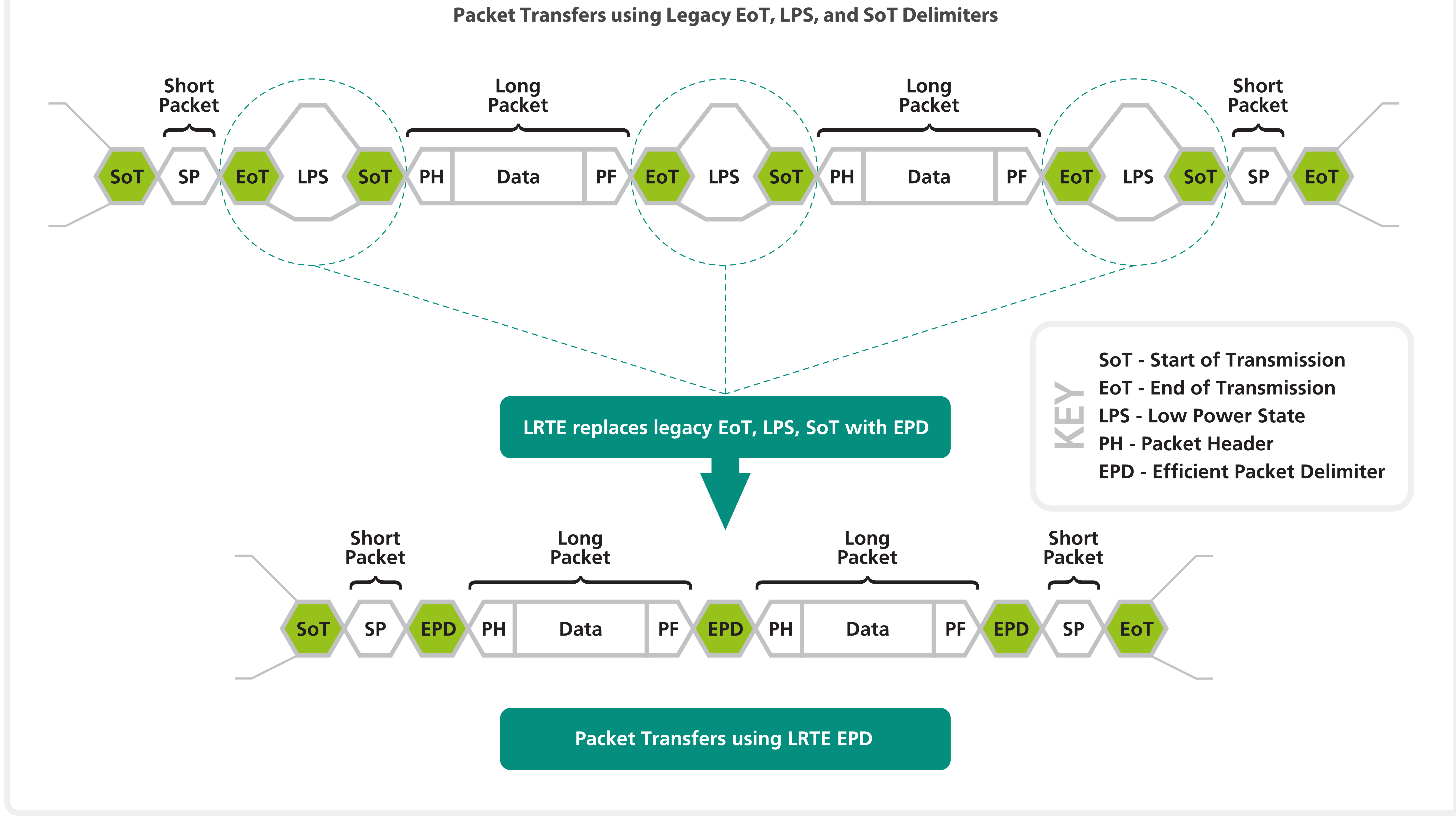
Figure 5. CSI-2 v2.0's LRTE (latency reduction transport efficiency) feature optimizes bandwidth utilization versus legacy approaches.
Also, in addressing electrical overstress that might normally be exhibited by the advanced process nodes now used to fabricate both image sensors and application processors, LRTE provides an optional alternate low-power signaling feature, along with a transition path to eventually phase out current high voltage (1.2 v) requirements.
The following system design example, summarized in Table 1, analyzes CSI-2 benefits when using LRTE PDQ, which supports popular 2.3 MPixel,/12 BBP (bit-per-pixel)/ 60 FPS (frame per second) automotive image sensors and reduces latency by more than 23% in comparison to continued use of legacy C-PHY packet delimiters.
Example system: CSI-2 v2.0 over C-PHY v1.2 (3.5 Gsps/lane, i.e. Gbps/lane)
- 24 Gbps using 3 lanes (requires 9 wires)
- CSI-2 v2.0 supports up to 32 VC over C-PHY
Multi-sensor aggregator with each image sensor configured as 1920×1200 pixels (2.3 Mpixels), 12 BPP, 60 FPS
Image sensor packet transport:
- 1,920 pixels x 12 bps = 23,040 bits per horizontal row LP (long packet)
- 23040 bits / 24 Gbps = 0.960 µs/LP (CSI-2 payload; ignoring packet header and footer)
PH (packet header) + PF (packet footer) = 336 bits + 48 bits= 384 bits - 23,424 bits / 24 Gbps = 0.976 µs /LP_PHF (CSI-2 payload with PH and PF)
CSI-2 v2.0 with legacy C-PHY packet delimiters:
- LP delimiter (SoT/EoT) = ~0.3 µs
- Total time per LP_PHF = 1.276 µs
- Packet delimiter overhead = 23.5%
- Time per image frame = 1.276 µs x 1,200 = 1.53 ms (ignoring FS/FE)
Streaming 60 frames from a single image sensor requires 1.53 ms x 60 = 91.87 ms
Maximum supported image sensors per aggregator = 10
FLOOR[1/0.09187] = FLOOR[10.88]
CSI-2 v2.0 with LRTE PDQ:
- Time per image frame = 0.976 µs x 1,200 = 1.171 ms
- Streaming 60 frames from a single image sensor requires 1.172ms x 60 = 70.27 ms
- Maximum supported image sensors per aggregator = 14
- FLOOR[1/0.07027] = FLOOR[14.23]
Benefits of CSI-2 v2.0 with LRTE PDQ:
- Frame transport efficiency improvement: 23.5%
- Additional supported image sensors on aggregator: +4 (over the same channel)
- Alternatively, you can reduce the toggle rate and/or number of wires
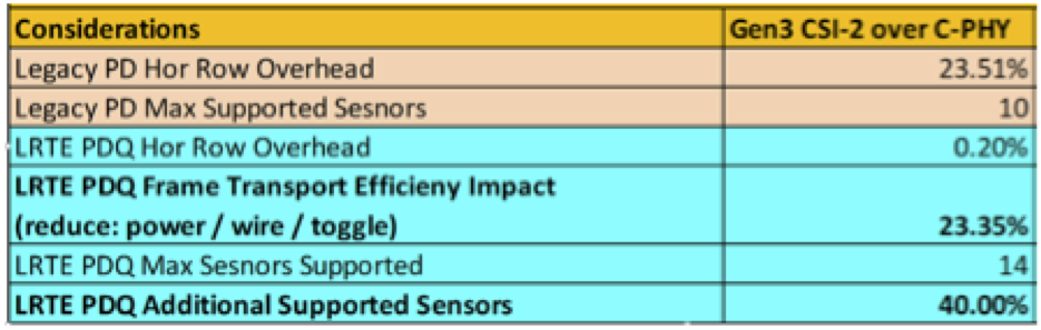
Table 1. Summary of design example efficiency and other improvements
DPCM 12-10-12
Leveraging the success of DPCM (differential pulse code modulation) 12-8-12 for data transfer purposes, DPCM 12-10-12 has subsequently been developed in order to further boost image quality (Figure 6). DPCM 12-10-12 reduces that maximum absolute error of a single-bit change in pixel value by a factor of 4.43x. Furthermore, the MTF (modulation transfer function) frequency response analysis closely tracks the original input, showing that the converted image is devoid of compression artifacts over various illumination and contrast combinations, therefore virtually indistinguishable from the original image.
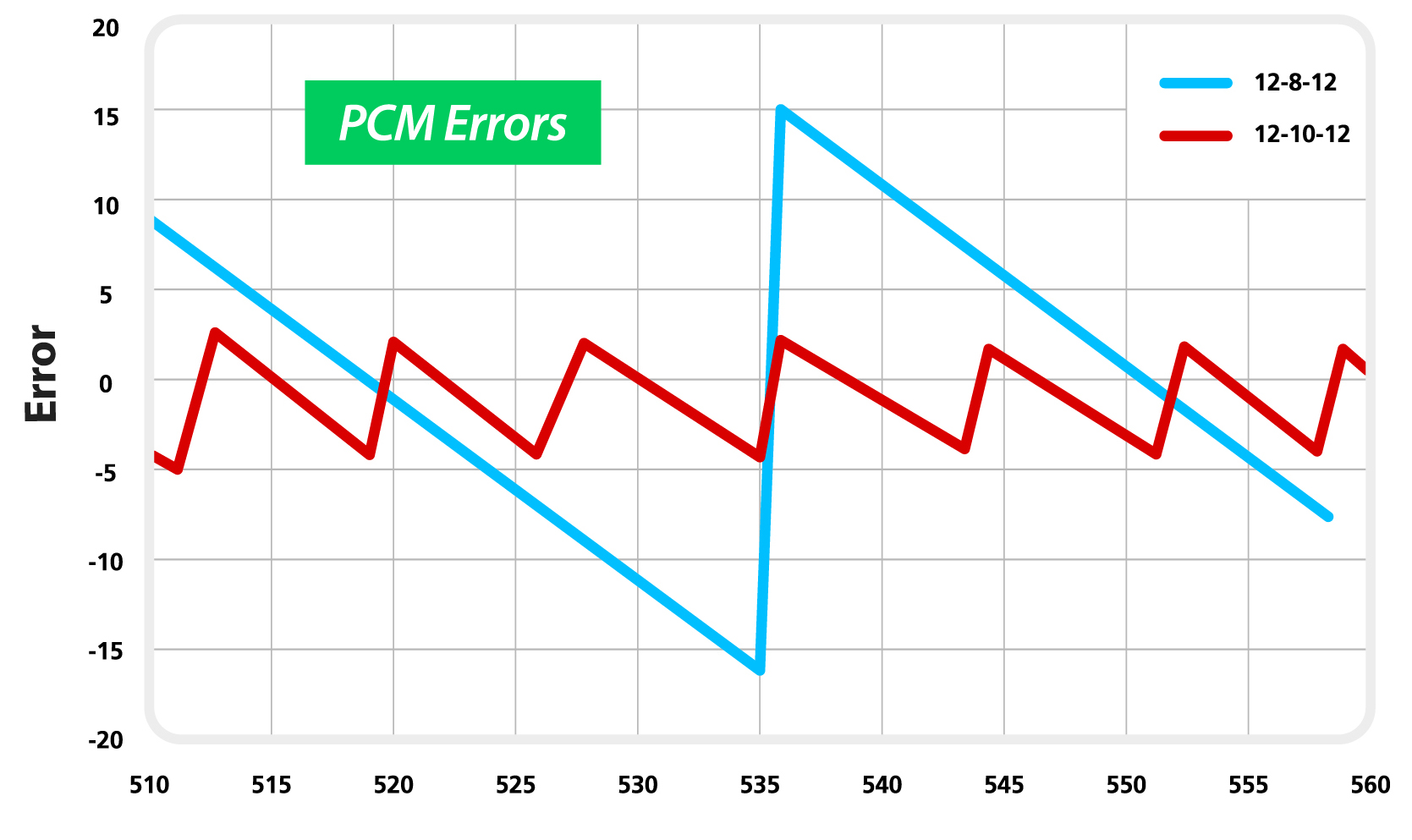
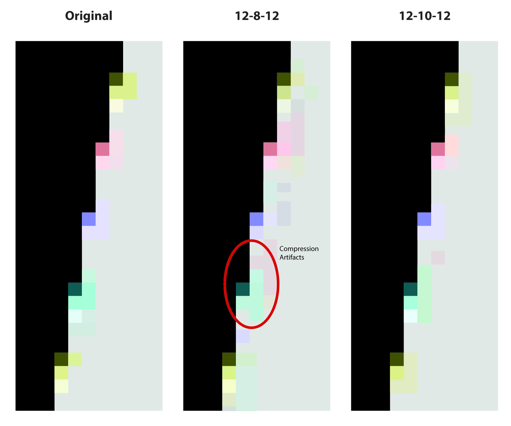
Figure 6. CSI-2 2.0's DPCM 12-10-12 reduces PCM errors by a factor of 4.43x (top) along with notably reducing compression artifacts (bottom) in comparison to prior-generation DPCM 12-8-12.
Table 2 illustrates the link bandwidth reduction and cost savings benefits of using CSI-2 DPCM for relatively popular imaging formats.
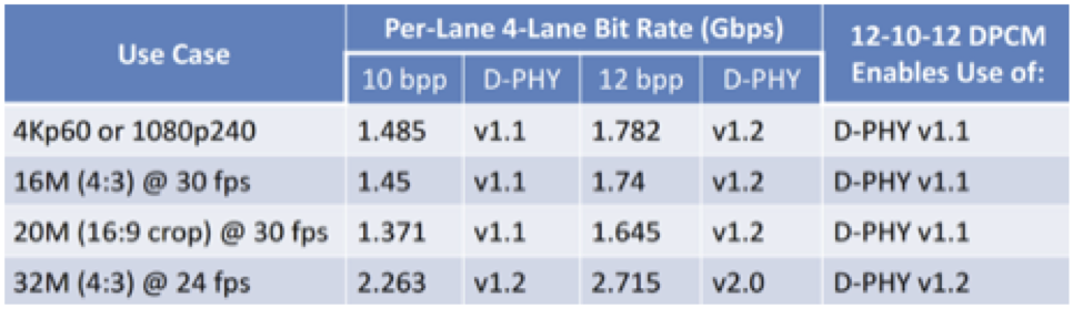
Table 2. Bandwidth reduction and cost savings for CSI-2 DPCM with various imaging formats.
An explanation of why DPCM is important follows: differential pulse code modulation provides compression while preserving object edges, devoid of lossy compression artifacts. This attribute is particularly useful for vision applications; recognizing characters on a street sign, for example. And the DPCM compression techniques are passed through a myriad of objective qualifications, such as high/medium/low contrast modular transfer function response testing.
Lowered Electromagnetic Interference
CSI-2 v2.0 supports Galois Field 2^16 scrambling to lower electromagnetic interference by reducing PSD (power spectral density) emissions across a broad range of frequencies, both for the CSI-2 over C-PHY channel (embedded clock and data) and the CSI-2 over D-PHY data lanes (Figure 7). Standard scrambling utilizes a lane-based seed reinitialized using the C/D-PHY Sync signals, while enhanced scrambling is provided for CSI-2 over C-PHY with unique Sync words.
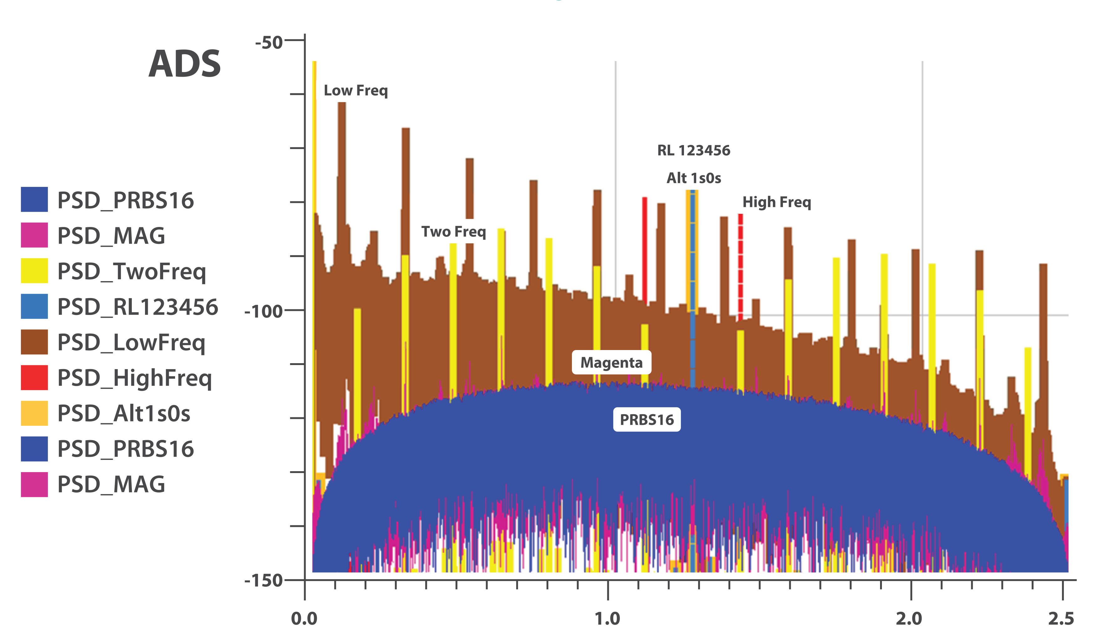
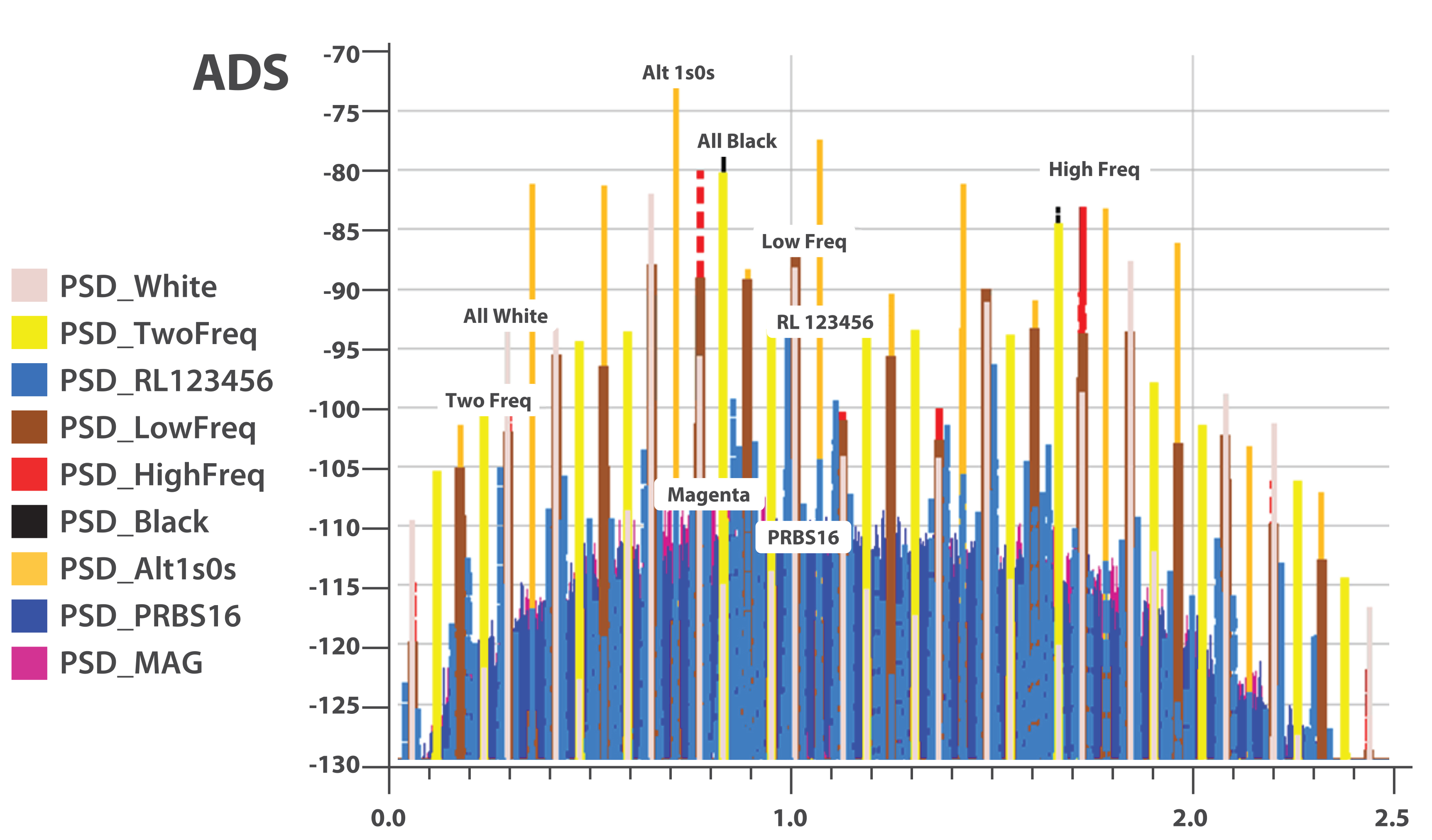
Figure 7. CSI-2 over D-PHY (top) and C-PHY (bottom) both exhibit decreased PSD (power spectral density) emissions when Galois Field scrambling is active.
Table 3 summarizes CSI-2 v2.0 imaging conduit capabilities.
|
CSI-2 v2.0 features |
Requires C-PHY v1.2? |
Requires D-PHY v2.1? |
Notes |
|
RAW-16 Improves intra-scene dynamic range |
No |
No |
Supports legacy C/D-PHYs |
|
RAW-20 Improves intra-scene dynamic range |
No |
No |
Supports legacy C/D-PHYs |
|
Galois Field 2^16 Scrambling Reduces PSD emissions |
Standard: No |
Standard: No Enhanced: Yes |
Supports Legacy C-PHY (embedded clock and data) and D-PHY (data lanes only). Enhanced SCR requires an updated C-PHY Sync detector |
|
LRTE PDQ Reduces latency, enhanced sensor aggregation, improves efficiency |
Preserve integrity: No |
Preserve integrity HS-Idle: Yes Drop integrity: No |
Maintain CSI PGCD integrity: Uses legacy C-PHY Sync Code. Requires new Gen3 D-PHY v2.1 HS-Idle
Drop CSI PCCD integrity: supports legacy D-PHY |
|
LRTE ALPS Transition path to reduce/eliminate 1.2V requirements |
ALP Codes: Yes |
LVLP: Yes |
Gen3 D-PHY v2.1 supports LVLP
Gen3 C-PHY v1.2 supports ALP Codes. C-PHY logic change is required, and LVLP is nice-to-have. |
|
DPCM 12-10-12 Reduce RAW-12 bandwidth while preserving SNR |
No |
No |
Supports legacy C/D-PHYs |
|
Virtual Channel Extension Sensor aggregation, Multi/HDR exposures along with IR support |
No (supports 32 VCs) |
No (supports 16 VCs) |
CSI-2 over C-PHY reuses RES with a path to 1024 VCs
CSI-2 over D-PHY requires new ECC logic to support 16 VCs |
|
Gen1 / Gen2 IOT Fixes ECC syndrome, embedded data interleave, lane de-skew and elastic store |
No |
No |
Fixes for issues identified in prior product-interoperability testing |
Table 3. CSI-2 v2.0 key features.
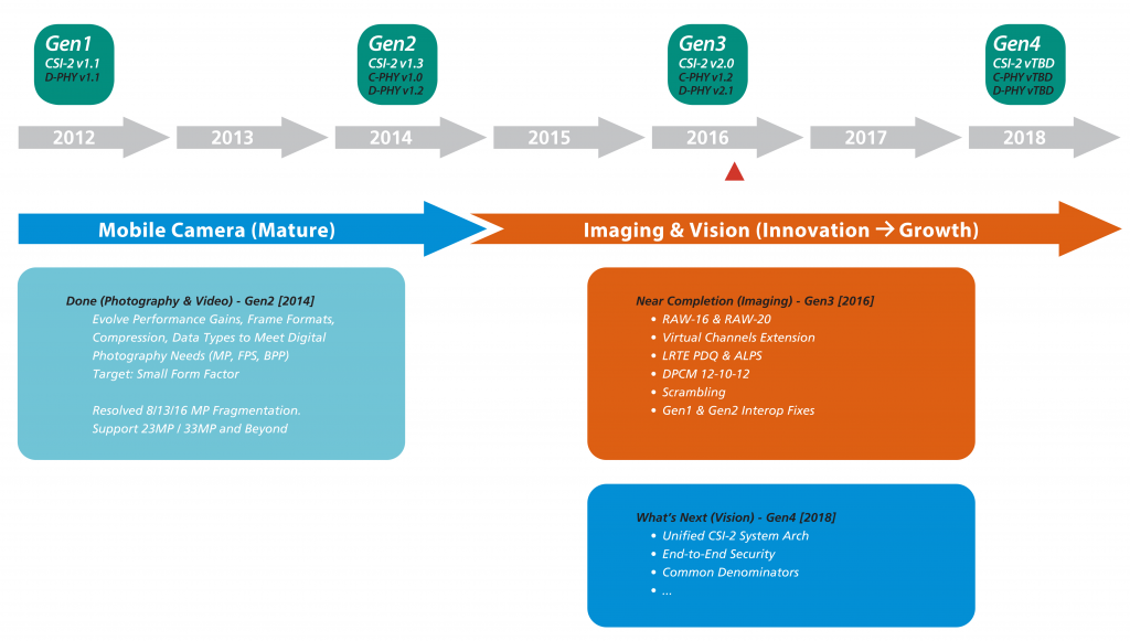
As previously mentioned, the MIPI Camera Working Group evolves CSI-2 at a two-year cadence (Figure 8). "Gen4" CSI-2, currently scheduled for finalization in 2018, will build on prior generation specifications with new features, potentially including:
- A unified CSI-2 system architecture, including an embedded Camera Command Interface, for long-reach applications.
- Architecture revisions to support end-to-end security, decoupled from the underlying PHY, SerDes, aggregators, repeaters, networks and other building blocks.
- Features common to machine learning and inference applications, including CNNs (convolutional neural networks) and HoG (the histogram of oriented gradients)
Such so-called "common denominators" encompass a broad array of provisions to aid imaging and vision applications. For instance, ARVR (Augmented Reality Virtual Reality) panels require support for extremely high resolution in order to deliver near-20/20 vision. One of the Gen4 CSI-2 common denominators that’s presently under consideration involves the inclusion of (x,y) coordinates for eye-tracking image sensors, sending this information as a CSI-2 data type using low latency (LRTE) mode to the graphics or other compute engine residing in an application processor. This engine could therefore conserve power by using reduced resources to generate high resolution content only in the limited area surrounding the (x,y) focal region.
For more information on CSI-2, including webinars, tutorials, and contact details, visit the MIPI CWG site at http://mipi.org/working-groups/camera.
Conclusion
Vision technology is enabling a wide range of products that are more intelligent and responsive than before, and thus more valuable to users. Vision processing can add valuable capabilities to existing products. And it can provide significant new markets for hardware, software and semiconductor suppliers (see sidebar "Additional Developer Assistance"). Reliably transferring still and video information from a camera or image sensor capture source to its processing destination is a critical aspect of any vision processing system design. Ever-increasing application demands for higher quality images at increasing resolutions and frame rates drive ongoing evolutions and revolutions in these interfaces, for both intra- and inter-system configurations.
Sidebar: Additional Developer Assistance
The Embedded Vision Alliance, a worldwide organization of technology developers and providers, is working to empower product creators to transform the potential of vision processing into reality. Allied Vision, Basler, Intel, videantis and Xilinx, the co-authors of this article, are members of the Embedded Vision Alliance; the MIPI Alliance is a valued partner organization. The Embedded Vision Alliance's mission is to provide product creators with practical education, information and insights to help them incorporate vision capabilities into new and existing products. To execute this mission, the Embedded Vision Alliance maintains a website providing tutorial articles, videos, code downloads and a discussion forum staffed by technology experts. Registered website users can also receive the Embedded Vision Alliance’s twice-monthly email newsletter, Embedded Vision Insights, among other benefits.
The Embedded Vision Alliance also offers a free online training facility for vision-based product creators: the Embedded Vision Academy. This area of the Embedded Vision Alliance website provides in-depth technical training and other resources to help product creators integrate visual intelligence into next-generation software and systems. Course material in the Embedded Vision Academy spans a wide range of vision-related subjects, from basic vision algorithms to image pre-processing, image sensor interfaces, and software development techniques and tools such as OpenCL, OpenVX and OpenCV, along with Caffe, TensorFlow and other deep learning frameworks. Access is free to all through a simple registration process.
The Embedded Vision Alliance’s annual technical conference and trade show, the Embedded Vision Summit, will be held May 1-3, 2017 at the Santa Clara, California Convention Center. Designed for product creators interested in incorporating visual intelligence into electronic systems and software, the Summit provides how-to presentations, inspiring keynote talks, demonstrations, and opportunities to interact with technical experts from Embedded Vision Alliance member companies. The Summit is intended to inspire attendees' imaginations about the potential applications for practical computer vision technology through exciting presentations and demonstrations, to offer practical know-how for attendees to help them incorporate vision capabilities into their hardware and software products, and to provide opportunities for attendees to meet and talk with leading vision technology companies and learn about their offerings. Online registration and additional information on the 2017 Embedded Vision Summit are now available.
By Brian Dipert
Editor-in-Chief, Embedded Vision Alliance
Michael Melle
Sales Development Manager, Allied Vision
Francis Obidimalor
Marketing Manager, Allied Vision
Mark Hebbel
Head of New Business Development, Basler
Frank Karstens
Product Manager, Basler
Haran Thanigasalam
Senior Platform Architect, Intel
Camera Workgroup Chairman, MIPI Alliance
Marco Jacobs
Vice President of Marketing, videantis
Aaron Behman
Director of Strategic Marketing for Embedded Vision, Xilinx